Операти́вная па́мять (англ. Random Access Memory, RAM, память с произвольным доступом) или операти́вное запомина́ющее устро́йство (ОЗУ); комп. жарг. па́мять, операти́вка — энергозависимая часть системы компьютерной памяти, в которой во время работы компьютера хранится выполняемый машинный код (программы), а также входные, выходные и промежуточные данные, обрабатываемые процессором.
Все значения словосочетания «оперативная память»
-
Как правило, у винчестера самый большой объём памяти, отличающийся на порядок, поэтому его легко отличить от объёма оперативной памяти компьютера и видеокарты.
-
Это делается для того, чтобы злоумышленнику было труднее получить доступ к критически важным данным, анализируя содержимое оперативной памяти компьютера.
-
Через них проходит огромный поток информации, поэтому упор у них делается на мощный процессор, большую оперативную память и большие жёсткие диски.
- (все предложения)
- модули памяти
- объём памяти
- виртуальная память
- расширенная память
- внешняя память
- (ещё синонимы…)
- память
- компьютер
- (ещё ассоциации…)
- оперативная группа
- в оперативный отдел штаба
- выйти на оперативный простор
- (полная таблица сочетаемости…)
- по старой памяти
- в памяти события
- из глубин памяти
- память подсказывала
- врезаться в память
- (полная таблица сочетаемости…)
- Разбор по составу слова «оперативный»
- Разбор по составу слова «память»
- Как правильно пишется слово «оперативный»
- Как правильно пишется слово «память»
«RAM» redirects here. For other uses, see Ram.


Random-access memory (RAM; ) is a form of computer memory that can be read and changed in any order, typically used to store working data and machine code.[1][2] A random-access memory device allows data items to be read or written in almost the same amount of time irrespective of the physical location of data inside the memory, in contrast with other direct-access data storage media (such as hard disks, CD-RWs, DVD-RWs and the older magnetic tapes and drum memory), where the time required to read and write data items varies significantly depending on their physical locations on the recording medium, due to mechanical limitations such as media rotation speeds and arm movement.
RAM contains multiplexing and demultiplexing circuitry, to connect the data lines to the addressed storage for reading or writing the entry. Usually more than one bit of storage is accessed by the same address, and RAM devices often have multiple data lines and are said to be «8-bit» or «16-bit», etc. devices.[clarification needed]
In today’s technology, random-access memory takes the form of integrated circuit (IC) chips with MOS (metal-oxide-semiconductor) memory cells. RAM is normally associated with volatile types of memory where stored information is lost if power is removed. The two main types of volatile random-access semiconductor memory are static random-access memory (SRAM) and dynamic random-access memory (DRAM).
Non-volatile RAM has also been developed[3]
and other types of non-volatile memories allow random access for read operations, but either do not allow write operations or have other kinds of limitations on them. These include most types of ROM and a type of flash memory called NOR-Flash.
Use of semiconductor RAM dated back to 1965, when IBM introduced the monolithic (single-chip) 16-bit SP95 SRAM chip for their System/360 Model 95 computer, and Toshiba used discrete DRAM memory cells for its 180-bit Toscal BC-1411 electronic calculator, both based on bipolar transistors. While it offered improved performance over magnetic-core memory, bipolar DRAM could not compete with the lower price of the then-dominant magnetic-core memory.[4]
MOS memory, based on MOS transistors, was developed in the late 1960s, and was the basis for all early commercial semiconductor memory. The first commercial DRAM IC chip, the 1K Intel 1103, was introduced in October 1970.
Synchronous dynamic random-access memory (SDRAM) later debuted with the Samsung KM48SL2000 chip in 1992.
History


Early computers used relays, mechanical counters[5] or delay lines for main memory functions. Ultrasonic delay lines were serial devices which could only reproduce data in the order it was written. Drum memory could be expanded at relatively low cost but efficient retrieval of memory items required knowledge of the physical layout of the drum to optimize speed. Latches built out of vacuum tube triodes, and later, out of discrete transistors, were used for smaller and faster memories such as registers. Such registers were relatively large and too costly to use for large amounts of data; generally only a few dozen or few hundred bits of such memory could be provided.
The first practical form of random-access memory was the Williams tube starting in 1947. It stored data as electrically charged spots on the face of a cathode-ray tube. Since the electron beam of the CRT could read and write the spots on the tube in any order, memory was random access. The capacity of the Williams tube was a few hundred to around a thousand bits, but it was much smaller, faster, and more power-efficient than using individual vacuum tube latches. Developed at the University of Manchester in England, the Williams tube provided the medium on which the first electronically stored program was implemented in the Manchester Baby computer, which first successfully ran a program on 21 June 1948.[6] In fact, rather than the Williams tube memory being designed for the Baby, the Baby was a testbed to demonstrate the reliability of the memory.[7][8]
Magnetic-core memory was invented in 1947 and developed up until the mid-1970s. It became a widespread form of random-access memory, relying on an array of magnetized rings. By changing the sense of each ring’s magnetization, data could be stored with one bit stored per ring. Since every ring had a combination of address wires to select and read or write it, access to any memory location in any sequence was possible. Magnetic core memory was the standard form of computer memory system until displaced by solid-state MOS (metal–oxide–silicon) semiconductor memory in integrated circuits (ICs) during the early 1970s.[9]
Prior to the development of integrated read-only memory (ROM) circuits, permanent (or read-only) random-access memory was often constructed using diode matrices driven by address decoders, or specially wound core rope memory planes.[citation needed]
Semiconductor memory began in the 1960s with bipolar memory, which used bipolar transistors. While it improved performance, it could not compete with the lower price of magnetic core memory.[10]
MOS RAM
The invention of the MOSFET (metal-oxide-semiconductor field-effect transistor), also known as the MOS transistor, by Mohamed M. Atalla and Dawon Kahng at Bell Labs in 1959,[11] led to the development of metal-oxide-semiconductor (MOS) memory by John Schmidt at Fairchild Semiconductor in 1964.[9][12] In addition to higher performance, MOS semiconductor memory was cheaper and consumed less power than magnetic core memory.[9] The development of silicon-gate MOS integrated circuit (MOS IC) technology by Federico Faggin at Fairchild in 1968 enabled the production of MOS memory chips.[13] MOS memory overtook magnetic core memory as the dominant memory technology in the early 1970s.[9]
An integrated bipolar static random-access memory (SRAM) was invented by Robert H. Norman at Fairchild Semiconductor in 1963.[14] It was followed by the development of MOS SRAM by John Schmidt at Fairchild in 1964.[9] SRAM became an alternative to magnetic-core memory, but required six MOS transistors for each bit of data.[15] Commercial use of SRAM began in 1965, when IBM introduced the SP95 memory chip for the System/360 Model 95.[10]
Dynamic random-access memory (DRAM) allowed replacement of a 4 or 6-transistor latch circuit by a single transistor for each memory bit, greatly increasing memory density at the cost of volatility. Data was stored in the tiny capacitance of each transistor, and had to be periodically refreshed every few milliseconds before the charge could leak away. Toshiba’s Toscal BC-1411 electronic calculator, which was introduced in 1965,[16][17][18] used a form of capacitive bipolar DRAM, storing 180-bit data on discrete memory cells, consisting of germanium bipolar transistors and capacitors.[17][18] While it offered improved performance over magnetic-core memory, bipolar DRAM could not compete with the lower price of the then dominant magnetic-core memory.[19]
MOS technology is the basis for modern DRAM. In 1966, Dr. Robert H. Dennard at the IBM Thomas J. Watson Research Center was working on MOS memory. While examining the characteristics of MOS technology, he found it was capable of building capacitors, and that storing a charge or no charge on the MOS capacitor could represent the 1 and 0 of a bit, while the MOS transistor could control writing the charge to the capacitor. This led to his development of a single-transistor DRAM memory cell.[15] In 1967, Dennard filed a patent under IBM for a single-transistor DRAM memory cell, based on MOS technology.[20] The first commercial DRAM IC chip was the Intel 1103, which was manufactured on an 8 µm MOS process with a capacity of 1 kbit, and was released in 1970.[9][21][22]
Synchronous dynamic random-access memory (SDRAM) was developed by Samsung Electronics. The first commercial SDRAM chip was the Samsung KM48SL2000, which had a capacity of 16 Mbit.[23] It was introduced by Samsung in 1992,[24] and mass-produced in 1993.[23] The first commercial DDR SDRAM (double data rate SDRAM) memory chip was Samsung’s 64 Mbit DDR SDRAM chip, released in June 1998.[25] GDDR (graphics DDR) is a form of DDR SGRAM (synchronous graphics RAM), which was first released by Samsung as a 16 Mbit memory chip in 1998.[26]
Types
The two widely used forms of modern RAM are static RAM (SRAM) and dynamic RAM (DRAM). In SRAM, a bit of data is stored using the state of a six-transistor memory cell, typically using six MOSFETs. This form of RAM is more expensive to produce, but is generally faster and requires less dynamic power than DRAM. In modern computers, SRAM is often used as cache memory for the CPU. DRAM stores a bit of data using a transistor and capacitor pair (typically a MOSFET and MOS capacitor, respectively),[27] which together comprise a DRAM cell. The capacitor holds a high or low charge (1 or 0, respectively), and the transistor acts as a switch that lets the control circuitry on the chip read the capacitor’s state of charge or change it. As this form of memory is less expensive to produce than static RAM, it is the predominant form of computer memory used in modern computers.
Both static and dynamic RAM are considered volatile, as their state is lost or reset when power is removed from the system. By contrast, read-only memory (ROM) stores data by permanently enabling or disabling selected transistors, such that the memory cannot be altered. Writeable variants of ROM (such as EEPROM and NOR flash) share properties of both ROM and RAM, enabling data to persist without power and to be updated without requiring special equipment. ECC memory (which can be either SRAM or DRAM) includes special circuitry to detect and/or correct random faults (memory errors) in the stored data, using parity bits or error correction codes.
In general, the term RAM refers solely to solid-state memory devices (either DRAM or SRAM), and more specifically the main memory in most computers. In optical storage, the term DVD-RAM is somewhat of a misnomer since, unlike CD-RW or DVD-RW it does not need to be erased before reuse. Nevertheless, a DVD-RAM behaves much like a hard disc drive if somewhat slower.
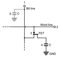
Memory cell
The memory cell is the fundamental building block of computer memory. The memory cell is an electronic circuit that stores one bit of binary information and it must be set to store a logic 1 (high voltage level) and reset to store a logic 0 (low voltage level). Its value is maintained/stored until it is changed by the set/reset process. The value in the memory cell can be accessed by reading it.
In SRAM, the memory cell is a type of flip-flop circuit, usually implemented using FETs. This means that SRAM requires very low power when not being accessed, but it is expensive and has low storage density.
A second type, DRAM, is based around a capacitor. Charging and discharging this capacitor can store a «1» or a «0» in the cell. However, the charge in this capacitor slowly leaks away, and must be refreshed periodically. Because of this refresh process, DRAM uses more power, but it can achieve greater storage densities and lower unit costs compared to SRAM.
|
SRAM Cell (6 Transistors) |
DRAM Cell (1 Transistor and one capacitor) |
Addressing
To be useful, memory cells must be readable and writeable. Within the RAM device, multiplexing and demultiplexing circuitry is used to select memory cells. Typically, a RAM device has a set of address lines A0… An, and for each combination of bits that may be applied to these lines, a set of memory cells are activated. Due to this addressing, RAM devices virtually always have a memory capacity that is a power of two.
Usually several memory cells share the same address. For example, a 4 bit ‘wide’ RAM chip has 4 memory cells for each address. Often the width of the memory and that of the microprocessor are different, for a 32 bit microprocessor, eight 4 bit RAM chips would be needed.
Often more addresses are needed than can be provided by a device. In that case, external multiplexors to the device are used to activate the correct device that is being accessed.
Memory hierarchy
One can read and over-write data in RAM. Many computer systems have a memory hierarchy consisting of processor registers, on-die SRAM caches, external caches, DRAM, paging systems and virtual memory or swap space on a hard drive. This entire pool of memory may be referred to as «RAM» by many developers, even though the various subsystems can have very different access times, violating the original concept behind the random access term in RAM. Even within a hierarchy level such as DRAM, the specific row, column, bank, rank, channel, or interleave organization of the components make the access time variable, although not to the extent that access time to rotating storage media or a tape is variable. The overall goal of using a memory hierarchy is to obtain the highest possible average access performance while minimizing the total cost of the entire memory system (generally, the memory hierarchy follows the access time with the fast CPU registers at the top and the slow hard drive at the bottom).
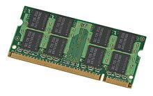
In many modern personal computers, the RAM comes in an easily upgraded form of modules called memory modules or DRAM modules about the size of a few sticks of chewing gum. These can quickly be replaced should they become damaged or when changing needs demand more storage capacity. As suggested above, smaller amounts of RAM (mostly SRAM) are also integrated in the CPU and other ICs on the motherboard, as well as in hard-drives, CD-ROMs, and several other parts of the computer system.
Other uses of RAM
In addition to serving as temporary storage and working space for the operating system and applications, RAM is used in numerous other ways.
Virtual memory
Most modern operating systems employ a method of extending RAM capacity, known as «virtual memory». A portion of the computer’s hard drive is set aside for a paging file or a scratch partition, and the combination of physical RAM and the paging file form the system’s total memory. (For example, if a computer has 2 GB (10243 B) of RAM and a 1 GB page file, the operating system has 3 GB total memory available to it.) When the system runs low on physical memory, it can «swap» portions of RAM to the paging file to make room for new data, as well as to read previously swapped information back into RAM. Excessive use of this mechanism results in thrashing and generally hampers overall system performance, mainly because hard drives are far slower than RAM.
RAM disk
Software can «partition» a portion of a computer’s RAM, allowing it to act as a much faster hard drive that is called a RAM disk. A RAM disk loses the stored data when the computer is shut down, unless memory is arranged to have a standby battery source, or changes to the RAM disk are written out to a nonvolatile disk. The RAM disk is reloaded from the physical disk upon RAM disk initialization.
Shadow RAM
Sometimes, the contents of a relatively slow ROM chip are copied to read/write memory to allow for shorter access times. The ROM chip is then disabled while the initialized memory locations are switched in on the same block of addresses (often write-protected). This process, sometimes called shadowing, is fairly common in both computers and embedded systems.
As a common example, the BIOS in typical personal computers often has an option called «use shadow BIOS» or similar. When enabled, functions that rely on data from the BIOS’s ROM instead use DRAM locations (most can also toggle shadowing of video card ROM or other ROM sections). Depending on the system, this may not result in increased performance, and may cause incompatibilities. For example, some hardware may be inaccessible to the operating system if shadow RAM is used. On some systems the benefit may be hypothetical because the BIOS is not used after booting in favor of direct hardware access. Free memory is reduced by the size of the shadowed ROMs.[28]
Recent developments
Several new types of non-volatile RAM, which preserve data while powered down, are under development. The technologies used include carbon nanotubes and approaches utilizing Tunnel magnetoresistance. Amongst the 1st generation MRAM, a 128 kbit (128 × 210 bytes) chip was manufactured with 0.18 µm technology in the summer of 2003.[citation needed] In June 2004, Infineon Technologies unveiled a 16 MB (16 × 220 bytes) prototype again based on 0.18 µm technology. There are two 2nd generation techniques currently in development: thermal-assisted switching (TAS)[29] which is being developed by Crocus Technology, and spin-transfer torque (STT) on which Crocus, Hynix, IBM, and several other companies are working.[30] Nantero built a functioning carbon nanotube memory prototype 10 GB (10 × 230 bytes) array in 2004. Whether some of these technologies can eventually take significant market share from either DRAM, SRAM, or flash-memory technology, however, remains to be seen.
Since 2006, «solid-state drives» (based on flash memory) with capacities exceeding 256 gigabytes and performance far exceeding traditional disks have become available. This development has started to blur the definition between traditional random-access memory and «disks», dramatically reducing the difference in performance.
Some kinds of random-access memory, such as «EcoRAM», are specifically designed for server farms, where low power consumption is more important than speed.[31]
Memory wall
The «memory wall» is the growing disparity of speed between CPU and memory outside the CPU chip. An important reason for this disparity is the limited communication bandwidth beyond chip boundaries, which is also referred to as bandwidth wall. From 1986 to 2000, CPU speed improved at an annual rate of 55% while memory speed only improved at 10%. Given these trends, it was expected that memory latency would become an overwhelming bottleneck in computer performance.[32]
CPU speed improvements slowed significantly partly due to major physical barriers and partly because current CPU designs have already hit the memory wall in some sense. Intel summarized these causes in a 2005 document.[33]
First of all, as chip geometries shrink and clock frequencies rise, the transistor leakage current increases, leading to excess power consumption and heat… Secondly, the advantages of higher clock speeds are in part negated by memory latency, since memory access times have not been able to keep pace with increasing clock frequencies. Third, for certain applications, traditional serial architectures are becoming less efficient as processors get faster (due to the so-called Von Neumann bottleneck), further undercutting any gains that frequency increases might otherwise buy. In addition, partly due to limitations in the means of producing inductance within solid state devices, resistance-capacitance (RC) delays in signal transmission are growing as feature sizes shrink, imposing an additional bottleneck that frequency increases don’t address.
The RC delays in signal transmission were also noted in «Clock Rate versus IPC: The End of the Road for Conventional Microarchitectures»[34] which projected a maximum of 12.5% average annual CPU performance improvement between 2000 and 2014.
A different concept is the processor-memory performance gap, which can be addressed by 3D integrated circuits that reduce the distance between the logic and memory aspects that are further apart in a 2D chip.[35] Memory subsystem design requires a focus on the gap, which is widening over time.[36] The main method of bridging the gap is the use of caches; small amounts of high-speed memory that houses recent operations and instructions nearby the processor, speeding up the execution of those operations or instructions in cases where they are called upon frequently. Multiple levels of caching have been developed to deal with the widening gap, and the performance of high-speed modern computers relies on evolving caching techniques.[37] There can be up to a 53% difference between the growth in speed of processor and the lagging speed of main memory access.[38]
Solid-state hard drives have continued to increase in speed, from ~400 Mbit/s via SATA3 in 2012 up to ~3 GB/s via NVMe/PCIe in 2018, closing the gap between RAM and hard disk speeds, although RAM continues to be an order of magnitude faster, with single-lane DDR4 3200 capable of 25 GB/s, and modern GDDR even faster. Fast, cheap, non-volatile solid state drives have replaced some functions formerly performed by RAM, such as holding certain data for immediate availability in server farms — 1 terabyte of SSD storage can be had for $200, while 1 TB of RAM would cost thousands of dollars.[39][40]
Timeline
SRAM
| Date of introduction | Chip name | Capacity (bits) | Access time | SRAM type | Manufacturer(s) | Process | MOSFET | Ref |
|---|---|---|---|---|---|---|---|---|
| March 1963 | — | 1-bit | ? | Bipolar (cell) | Fairchild | — | — | [10] |
| 1965 | ? | 8-bit | ? | Bipolar | IBM | ? | — | |
| SP95 | 16-bit | ? | Bipolar | IBM | ? | — | [41] | |
| ? | 64-bit | ? | MOSFET | Fairchild | ? | PMOS | [42] | |
| 1966 | TMC3162 | 16-bit | ? | Bipolar (TTL) | Transitron | ? | — | [9] |
| ? | ? | ? | MOSFET | NEC | ? | ? | [43] | |
| 1968 | ? | 64-bit | ? | MOSFET | Fairchild | ? | PMOS | [43] |
| 144-bit | ? | MOSFET | NEC | ? | NMOS | |||
| 512-bit | ? | MOSFET | IBM | ? | NMOS | [42] | ||
| 1969 | ? | 128-bit | ? | Bipolar | IBM | ? | — | [10] |
| 1101 | 256-bit | 850 ns | MOSFET | Intel | 12,000 nm | PMOS | [44][45][46][47] | |
| 1972 | 2102 | 1 kbit | ? | MOSFET | Intel | ? | NMOS | [44] |
| 1974 | 5101 | 1 kbit | 800 ns | MOSFET | Intel | ? | CMOS | [44][48] |
| 2102A | 1 kbit | 350 ns | MOSFET | Intel | ? | NMOS (depletion) | [44][49] | |
| 1975 | 2114 | 4 kbit | 450 ns | MOSFET | Intel | ? | NMOS | [44][48] |
| 1976 | 2115 | 1 kbit | 70 ns | MOSFET | Intel | ? | NMOS (HMOS) | [44][45] |
| 2147 | 4 kbit | 55 ns | MOSFET | Intel | ? | NMOS (HMOS) | [44][50] | |
| 1977 | ? | 4 kbit | ? | MOSFET | Toshiba | ? | CMOS | [45] |
| 1978 | HM6147 | 4 kbit | 55 ns | MOSFET | Hitachi | 3,000 nm | CMOS (twin-well) | [50] |
| TMS4016 | 16 kbit | ? | MOSFET | Texas Instruments | ? | NMOS | [45] | |
| 1980 | ? | 16 kbit | ? | MOSFET | Hitachi, Toshiba | ? | CMOS | [51] |
| 64 kbit | ? | MOSFET | Matsushita | |||||
| 1981 | ? | 16 kbit | ? | MOSFET | Texas Instruments | 2,500 nm | NMOS | [51] |
| October 1981 | ? | 4 kbit | 18 ns | MOSFET | Matsushita, Toshiba | 2,000 nm | CMOS | [52] |
| 1982 | ? | 64 kbit | ? | MOSFET | Intel | 1,500 nm | NMOS (HMOS) | [51] |
| February 1983 | ? | 64 kbit | 50 ns | MOSFET | Mitsubishi | ? | CMOS | [53] |
| 1984 | ? | 256 kbit | ? | MOSFET | Toshiba | 1,200 nm | CMOS | [51][46] |
| 1987 | ? | 1 Mbit | ? | MOSFET | Sony, Hitachi, Mitsubishi, Toshiba | ? | CMOS | [51] |
| December 1987 | ? | 256 kbit | 10 ns | BiMOS | Texas Instruments | 800 nm | BiCMOS | [54] |
| 1990 | ? | 4 Mbit | 15–23 ns | MOSFET | NEC, Toshiba, Hitachi, Mitsubishi | ? | CMOS | [51] |
| 1992 | ? | 16 Mbit | 12–15 ns | MOSFET | Fujitsu, NEC | 400 nm | ||
| December 1994 | ? | 512 kbit | 2.5 ns | MOSFET | IBM | ? | CMOS (SOI) | [55] |
| 1995 | ? | 4 Mbit | 6 ns | Cache (SyncBurst) | Hitachi | 100 nm | CMOS | [56] |
| 256 Mbit | ? | MOSFET | Hyundai | ? | CMOS | [57] |
DRAM
| Date of introduction | Chip name | Capacity (bits) | DRAM type | Manufacturer(s) | Process | MOSFET | Area | Ref |
|---|---|---|---|---|---|---|---|---|
| 1965 | — | 1 bit | DRAM (cell) | Toshiba | — | — | — | [17][18] |
| 1967 | — | 1 bit | DRAM (cell) | IBM | — | MOS | — | [20][43] |
| 1968 | ? | 256 bit | DRAM (IC) | Fairchild | ? | PMOS | ? | [9] |
| 1969 | — | 1 bit | DRAM (cell) | Intel | — | PMOS | — | [43] |
| 1970 | 1102 | 1 kbit | DRAM (IC) | Intel, Honeywell | ? | PMOS | ? | [43] |
| 1103 | 1 kbit | DRAM | Intel | 8,000 nm | PMOS | 10 mm² | [58][59][21] | |
| 1971 | μPD403 | 1 kbit | DRAM | NEC | ? | NMOS | ? | [60] |
| ? | 2 kbit | DRAM | General Instrument | ? | PMOS | 13 mm² | [61] | |
| 1972 | 2107 | 4 kbit | DRAM | Intel | ? | NMOS | ? | [44][62] |
| 1973 | ? | 8 kbit | DRAM | IBM | ? | PMOS | 19 mm² | [61] |
| 1975 | 2116 | 16 kbit | DRAM | Intel | ? | NMOS | ? | [63][9] |
| 1977 | ? | 64 kbit | DRAM | NTT | ? | NMOS | 35 mm² | [61] |
| 1979 | MK4816 | 16 kbit | PSRAM | Mostek | ? | NMOS | ? | [64] |
| ? | 64 kbit | DRAM | Siemens | ? | VMOS | 25 mm² | [61] | |
| 1980 | ? | 256 kbit | DRAM | NEC, NTT | 1,000–1,500 nm | NMOS | 34–42 mm² | [61] |
| 1981 | ? | 288 kbit | DRAM | IBM | ? | MOS | 25 mm² | [65] |
| 1983 | ? | 64 kbit | DRAM | Intel | 1,500 nm | CMOS | 20 mm² | [61] |
| 256 kbit | DRAM | NTT | ? | CMOS | 31 mm² | |||
| January 5, 1984 | ? | 8 Mbit | DRAM | Hitachi | ? | MOS | ? | [66][67] |
| February 1984 | ? | 1 Mbit | DRAM | Hitachi, NEC | 1,000 nm | NMOS | 74–76 mm² | [61][68] |
| NTT | 800 nm | CMOS | 53 mm² | [61][68] | ||||
| 1984 | TMS4161 | 64 kbit | DPRAM (VRAM) | Texas Instruments | ? | NMOS | ? | [69][70] |
| January 1985 | μPD41264 | 256 kbit | DPRAM (VRAM) | NEC | ? | NMOS | ? | [71][72] |
| June 1986 | ? | 1 Mbit | PSRAM | Toshiba | ? | CMOS | ? | [73] |
| 1986 | ? | 4 Mbit | DRAM | NEC | 800 nm | NMOS | 99 mm² | [61] |
| Texas Instruments, Toshiba | 1,000 nm | CMOS | 100–137 mm² | |||||
| 1987 | ? | 16 Mbit | DRAM | NTT | 700 nm | CMOS | 148 mm² | [61] |
| October 1988 | ? | 512 kbit | HSDRAM | IBM | 1,000 nm | CMOS | 78 mm² | [74] |
| 1991 | ? | 64 Mbit | DRAM | Matsushita, Mitsubishi, Fujitsu, Toshiba | 400 nm | CMOS | ? | [51] |
| 1993 | ? | 256 Mbit | DRAM | Hitachi, NEC | 250 nm | CMOS | ? | |
| 1995 | ? | 4 Mbit | DPRAM (VRAM) | Hitachi | ? | CMOS | ? | [56] |
| January 9, 1995 | ? | 1 Gbit | DRAM | NEC | 250 nm | CMOS | ? | [75][56] |
| Hitachi | 160 nm | CMOS | ? | |||||
| 1996 | ? | 4 Mbit | FRAM | Samsung | ? | NMOS | ? | [76] |
| 1997 | ? | 4 Gbit | QLC | NEC | 150 nm | CMOS | ? | [51] |
| 1998 | ? | 4 Gbit | DRAM | Hyundai | ? | CMOS | ? | [57] |
| June 2001 | TC51W3216XB | 32 Mbit | PSRAM | Toshiba | ? | CMOS | ? | [77] |
| February 2001 | ? | 4 Gbit | DRAM | Samsung | 100 nm | CMOS | ? | [51][78] |
SDRAM
| Date of introduction | Chip name | Capacity (bits)[79] | SDRAM type | Manufacturer(s) | Process | MOSFET | Area | Ref |
|---|---|---|---|---|---|---|---|---|
| 1992 | KM48SL2000 | 16 Mbit | SDR | Samsung | ? | CMOS | ? | [80][23] |
| 1996 | MSM5718C50 | 18 Mbit | RDRAM | Oki | ? | CMOS | 325 mm2 | [81] |
| N64 RDRAM | 36 Mbit | RDRAM | NEC | ? | CMOS | ? | [82] | |
| ? | 1024 Mbit | SDR | Mitsubishi | 150 nm | CMOS | ? | [51] | |
| 1997 | ? | 1024 Mbit | SDR | Hyundai | ? | SOI | ? | [57] |
| 1998 | MD5764802 | 64 Mbit | RDRAM | Oki | ? | CMOS | 325 mm2 | [81] |
| March 1998 | Direct RDRAM | 72 Mbit | RDRAM | Rambus | ? | CMOS | ? | [83] |
| June 1998 | ? | 64 Mbit | DDR | Samsung | ? | CMOS | ? | [84][85][86] |
| 1998 | ? | 64 Mbit | DDR | Hyundai | ? | CMOS | ? | [57] |
| 128 Mbit | SDR | Samsung | ? | CMOS | ? | [87][85] | ||
| 1999 | ? | 128 Mbit | DDR | Samsung | ? | CMOS | ? | [85] |
| 1024 Mbit | DDR | Samsung | 140 nm | CMOS | ? | [51] | ||
| 2000 | GS eDRAM | 32 Mbit | eDRAM | Sony, Toshiba | 180 nm | CMOS | 279 mm2 | [88] |
| 2001 | ? | 288 Mbit | RDRAM | Hynix | ? | CMOS | ? | [89] |
| ? | DDR2 | Samsung | 100 nm | CMOS | ? | [86][51] | ||
| 2002 | ? | 256 Mbit | SDR | Hynix | ? | CMOS | ? | [89] |
| 2003 | EE+GS eDRAM | 32 Mbit | eDRAM | Sony, Toshiba | 90 nm | CMOS | 86 mm2 | [88] |
| ? | 72 Mbit | DDR3 | Samsung | 90 nm | CMOS | ? | [90] | |
| 512 Mbit | DDR2 | Hynix | ? | CMOS | ? | [89] | ||
| Elpida | 110 nm | CMOS | ? | [91] | ||||
| 1024 Mbit | DDR2 | Hynix | ? | CMOS | ? | [89] | ||
| 2004 | ? | 2048 Mbit | DDR2 | Samsung | 80 nm | CMOS | ? | [92] |
| 2005 | EE+GS eDRAM | 32 Mbit | eDRAM | Sony, Toshiba | 65 nm | CMOS | 86 mm2 | [93] |
| Xenos eDRAM | 80 Mbit | eDRAM | NEC | 90 nm | CMOS | ? | [94] | |
| ? | 512 Mbit | DDR3 | Samsung | 80 nm | CMOS | ? | [86][95] | |
| 2006 | ? | 1024 Mbit | DDR2 | Hynix | 60 nm | CMOS | ? | [89] |
| 2008 | ? | ? | LPDDR2 | Hynix | ? | |||
| April 2008 | ? | 8192 Mbit | DDR3 | Samsung | 50 nm | CMOS | ? | [96] |
| 2008 | ? | 16384 Mbit | DDR3 | Samsung | 50 nm | CMOS | ? | |
| 2009 | ? | ? | DDR3 | Hynix | 44 nm | CMOS | ? | [89] |
| 2048 Mbit | DDR3 | Hynix | 40 nm | |||||
| 2011 | ? | 16384 Mbit | DDR3 | Hynix | 40 nm | CMOS | ? | [97] |
| 2048 Mbit | DDR4 | Hynix | 30 nm | CMOS | ? | [97] | ||
| 2013 | ? | ? | LPDDR4 | Samsung | 20 nm | CMOS | ? | [97] |
| 2014 | ? | 8192 Mbit | LPDDR4 | Samsung | 20 nm | CMOS | ? | [98] |
| 2015 | ? | 12 Gbit | LPDDR4 | Samsung | 20 nm | CMOS | ? | [87] |
| 2018 | ? | 8192 Mbit | LPDDR5 | Samsung | 10 nm | FinFET | ? | [99] |
| 128 Gbit | DDR4 | Samsung | 10 nm | FinFET | ? | [100] |
SGRAM and HBM
| Date of introduction | Chip name | Capacity (bits)[79] | SDRAM type | Manufacturer(s) | Process | MOSFET | Area | Ref |
|---|---|---|---|---|---|---|---|---|
| November 1994 | HM5283206 | 8 Mbit | SGRAM (SDR) | Hitachi | 350 nm | CMOS | 58 mm2 | [101][102] |
| December 1994 | μPD481850 | 8 Mbit | SGRAM (SDR) | NEC | ? | CMOS | 280 mm2 | [103][104] |
| 1997 | μPD4811650 | 16 Mbit | SGRAM (SDR) | NEC | 350 nm | CMOS | 280 mm2 | [105][106] |
| September 1998 | ? | 16 Mbit | SGRAM (GDDR) | Samsung | ? | CMOS | ? | [84] |
| 1999 | KM4132G112 | 32 Mbit | SGRAM (SDR) | Samsung | ? | CMOS | ? | [107] |
| 2002 | ? | 128 Mbit | SGRAM (GDDR2) | Samsung | ? | CMOS | ? | [108] |
| 2003 | ? | 256 Mbit | SGRAM (GDDR2) | Samsung | ? | CMOS | ? | [108] |
| SGRAM (GDDR3) | ||||||||
| March 2005 | K4D553238F | 256 Mbit | SGRAM (GDDR) | Samsung | ? | CMOS | 77 mm2 | [109] |
| October 2005 | ? | 256 Mbit | SGRAM (GDDR4) | Samsung | ? | CMOS | ? | [110] |
| 2005 | ? | 512 Mbit | SGRAM (GDDR4) | Hynix | ? | CMOS | ? | [89] |
| 2007 | ? | 1024 Mbit | SGRAM (GDDR5) | Hynix | 60 nm | |||
| 2009 | ? | 2048 Mbit | SGRAM (GDDR5) | Hynix | 40 nm | |||
| 2010 | K4W1G1646G | 1024 Mbit | SGRAM (GDDR3) | Samsung | ? | CMOS | 100 mm2 | [111] |
| 2012 | ? | 4096 Mbit | SGRAM (GDDR3) | SK Hynix | ? | CMOS | ? | [97] |
| 2013 | ? | ? | HBM | |||||
| March 2016 | MT58K256M32JA | 8 Gbit | SGRAM (GDDR5X) | Micron | 20 nm | CMOS | 140 mm2 | [112] |
| June 2016 | ? | 32 Gbit | HBM2 | Samsung | 20 nm | CMOS | ? | [113][114] |
| 2017 | ? | 64 Gbit | HBM2 | Samsung | 20 nm | CMOS | ? | [113] |
| January 2018 | K4ZAF325BM | 16 Gbit | SGRAM (GDDR6) | Samsung | 10 nm | FinFET | 225 mm2 | [115][116][117] |
See also
- CAS latency (CL)
- Hybrid Memory Cube
- Multi-channel memory architecture
- Registered/buffered memory
- RAM parity
- Memory Interconnect/RAM buses
- Memory geometry
- Chip creep
- Read-mostly memory (RMM)
- Electrochemical random-access memory
References
- ^ «RAM». Cambridge English Dictionary. Retrieved 11 July 2019.
- ^ «RAM». Oxford Advanced Learner’s Dictionary. Retrieved 11 July 2019.
- ^ Gallagher, Sean (April 4, 2013). «Memory that never forgets: non-volatile DIMMs hit the market». Ars Technica. Archived from the original on July 8, 2017.
- ^ «1966: Semiconductor RAMs Serve High-speed Storage Needs». Computer History Museum.
- ^ «IBM Archives — FAQ’s for Products and Services». ibm.com. Archived from the original on 2012-10-23.
- ^ Napper, Brian, Computer 50: The University of Manchester Celebrates the Birth of the Modern Computer, archived from the original on 4 May 2012, retrieved 26 May 2012
- ^ Williams, F. C.; Kilburn, T. (Sep 1948), «Electronic Digital Computers», Nature, 162 (4117): 487, Bibcode:1948Natur.162..487W, doi:10.1038/162487a0, S2CID 4110351. Reprinted in The Origins of Digital Computers.
- ^ Williams, F. C.; Kilburn, T.; Tootill, G. C. (Feb 1951), «Universal High-Speed Digital Computers: A Small-Scale Experimental Machine», Proc. IEE, 98 (61): 13–28, doi:10.1049/pi-2.1951.0004, archived from the original on 2013-11-17.
- ^ a b c d e f g h i «1970: Semiconductors compete with magnetic cores». Computer History Museum. Retrieved 19 June 2019.
- ^ a b c d «1966: Semiconductor RAMs Serve High-speed Storage Needs». Computer History Museum. Retrieved 19 June 2019.
- ^ «1960 – Metal Oxide Semiconductor (MOS) Transistor Demonstrated». The Silicon Engine. Computer History Museum.
- ^ Solid State Design – Vol. 6. Horizon House. 1965.
- ^ «1968: Silicon Gate Technology Developed for ICs». Computer History Museum. Retrieved 10 August 2019.
- ^ US patent 3562721, Robert H. Norman, «Solid State Switching and Memory Apparatus», published 9 February1971
- ^ a b «DRAM». IBM100. IBM. 9 August 2017. Retrieved 20 September 2019.
- ^ Toscal BC-1411 calculator. Archived 2017-07-29 at the Wayback Machine, Science Museum, London.
- ^ a b c «Spec Sheet for Toshiba «TOSCAL» BC-1411″. Old Calculator Web Museum. Archived from the original on 3 July 2017. Retrieved 8 May 2018.
- ^ a b c Toshiba «Toscal» BC-1411 Desktop Calculator Archived 2007-05-20 at the Wayback Machine
- ^ «1966: Semiconductor RAMs Serve High-speed Storage Needs». Computer History Museum.
- ^ a b «Robert Dennard». Encyclopedia Britannica. Retrieved 8 July 2019.
- ^ a b Lojek, Bo (2007). History of Semiconductor Engineering. Springer Science & Business Media. pp. 362–363. ISBN 9783540342588.
The i1103 was manufactured on a 6-mask silicon-gate P-MOS process with 8 μm minimum features. The resulting product had a 2,400 µm² memory cell size, a die size just under 10 mm², and sold for around $21.
- ^ Bellis, Mary. «The Invention of the Intel 1103».
- ^ a b c «Electronic Design». Electronic Design. Hayden Publishing Company. 41 (15–21). 1993.
The first commercial synchronous DRAM, the Samsung 16-Mbit KM48SL2000, employs a single-bank architecture that lets system designers easily transition from asynchronous to synchronous systems.
- ^ «KM48SL2000-7 Datasheet». Samsung. August 1992. Retrieved 19 June 2019.
- ^ «Samsung Electronics Develops First 128Mb SDRAM with DDR/SDR Manufacturing Option». Samsung Electronics. Samsung. 10 February 1999. Retrieved 23 June 2019.
- ^ «Samsung Electronics Comes Out with Super-Fast 16M DDR SGRAMs». Samsung Electronics. Samsung. 17 September 1998. Retrieved 23 June 2019.
- ^ Sze, Simon M. (2002). Semiconductor Devices: Physics and Technology (PDF) (2nd ed.). Wiley. p. 214. ISBN 0-471-33372-7.
- ^ «Shadow Ram». Archived from the original on 2006-10-29. Retrieved 2007-07-24.
- ^ The Emergence of Practical MRAM «Crocus Technology | Magnetic Sensors | TMR Sensors» (PDF). Archived from the original (PDF) on 2011-04-27. Retrieved 2009-07-20.
- ^ «Tower invests in Crocus, tips MRAM foundry deal». EETimes. Archived from the original on 2012-01-19.
- ^
«EcoRAM held up as less power-hungry option than DRAM for server farms» Archived 2008-06-30 at the Wayback Machine
by Heather Clancy 2008 - ^ The term was coined in «Archived copy» (PDF). Archived (PDF) from the original on 2012-04-06. Retrieved 2011-12-14.
{{cite web}}: CS1 maint: archived copy as title (link). - ^ «Platform 2015: Intel® Processor and Platform Evolution for the Next Decade» (PDF). March 2, 2005. Archived (PDF) from the original on April 27, 2011.
- ^ Agarwal, Vikas; Hrishikesh, M. S.; Keckler, Stephen W.; Burger, Doug (June 10–14, 2000). «Clock Rate versus IPC: The End of the Road for Conventional Microarchitectures» (PDF). Proceedings of the 27th Annual International Symposium on Computer Architecture. 27th Annual International Symposium on Computer Architecture. Vancouver, BC. Retrieved 14 July 2018.
- ^ Rainer Waser (2012). Nanoelectronics and Information Technology. John Wiley & Sons. p. 790. ISBN 9783527409273. Archived from the original on August 1, 2016. Retrieved March 31, 2014.
- ^ Chris Jesshope and Colin Egan (2006). Advances in Computer Systems Architecture: 11th Asia-Pacific Conference, ACSAC 2006, Shanghai, China, September 6-8, 2006, Proceedings. Springer. p. 109. ISBN 9783540400561. Archived from the original on August 1, 2016. Retrieved March 31, 2014.
- ^ Ahmed Amine Jerraya and Wayne Wolf (2005). Multiprocessor Systems-on-chips. Morgan Kaufmann. pp. 90–91. ISBN 9780123852519. Archived from the original on August 1, 2016. Retrieved March 31, 2014.
- ^ Celso C. Ribeiro and Simone L. Martins (2004). Experimental and Efficient Algorithms: Third International Workshop, WEA 2004, Angra Dos Reis, Brazil, May 25-28, 2004, Proceedings, Volume 3. Springer. p. 529. ISBN 9783540220671. Archived from the original on August 1, 2016. Retrieved March 31, 2014.
- ^ «SSD Prices Continue to Fall, Now Upgrade Your Hard Drive!». MiniTool. 2018-09-03. Retrieved 2019-03-28.
- ^ Coppock, Mark (31 January 2017). «If you’re buying or upgrading your PC, expect to pay more for RAM». www.digitaltrends.com. Retrieved 2019-03-28.
- ^ IBM first in IC memory. Computer History Museum. IBM Corporation. 1965. Retrieved 19 June 2019.
- ^ a b Sah, Chih-Tang (October 1988). «Evolution of the MOS transistor-from conception to VLSI» (PDF). Proceedings of the IEEE. 76 (10): 1280–1326 (1303). Bibcode:1988IEEEP..76.1280S. doi:10.1109/5.16328. ISSN 0018-9219.
- ^ a b c d e «Late 1960s: Beginnings of MOS memory» (PDF). Semiconductor History Museum of Japan. 2019-01-23. Retrieved 27 June 2019.
- ^ a b c d e f g h «A chronological list of Intel products. The products are sorted by date» (PDF). Intel museum. Intel Corporation. July 2005. Archived from the original (PDF) on August 9, 2007. Retrieved July 31, 2007.
- ^ a b c d «1970s: SRAM evolution» (PDF). Semiconductor History Museum of Japan. Retrieved 27 June 2019.
- ^ a b Pimbley, J. (2012). Advanced CMOS Process Technology. Elsevier. p. 7. ISBN 9780323156806.
- ^ «Intel Memory». Intel Vintage. Retrieved 2019-07-06.
- ^ a b Component Data Catalog (PDF). Intel. 1978. p. 3. Retrieved 27 June 2019.
- ^ «Silicon Gate MOS 2102A». Intel. Retrieved 27 June 2019.
- ^ a b «1978: Double-well fast CMOS SRAM (Hitachi)» (PDF). Semiconductor History Museum of Japan. Retrieved 5 July 2019.
- ^ a b c d e f g h i j k l «Memory». STOL (Semiconductor Technology Online). Retrieved 25 June 2019.
- ^ Isobe, Mitsuo; Uchida, Yukimasa; Maeguchi, Kenji; Mochizuki, T.; Kimura, M.; Hatano, H.; Mizutani, Y.; Tango, H. (October 1981). «An 18 ns CMOS/SOS 4K static RAM». IEEE Journal of Solid-State Circuits. 16 (5): 460–465. Bibcode:1981IJSSC..16..460I. doi:10.1109/JSSC.1981.1051623. S2CID 12992820.
- ^ Yoshimoto, M.; Anami, K.; Shinohara, H.; Yoshihara, T.; Takagi, H.; Nagao, S.; Kayano, S.; Nakano, T. (1983). «A 64Kb full CMOS RAM with divided word line structure». 1983 IEEE International Solid-State Circuits Conference. Digest of Technical Papers. XXVI: 58–59. doi:10.1109/ISSCC.1983.1156503. S2CID 34837669.
- ^ Havemann, Robert H.; Eklund, R. E.; Tran, Hiep V.; Haken, R. A.; Scott, D. B.; Fung, P. K.; Ham, T. E.; Favreau, D. P.; Virkus, R. L. (December 1987). «An 0.8 #181;m 256K BiCMOS SRAM technology». 1987 International Electron Devices Meeting: 841–843. doi:10.1109/IEDM.1987.191564. S2CID 40375699.
- ^ Shahidi, Ghavam G.; Davari, Bijan; Dennard, Robert H.; Anderson, C. A.; Chappell, B. A.; et al. (December 1994). «A room temperature 0.1 µm CMOS on SOI». IEEE Transactions on Electron Devices. 41 (12): 2405–2412. Bibcode:1994ITED…41.2405S. doi:10.1109/16.337456. S2CID 108832941.
- ^ a b c «Japanese Company Profiles» (PDF). Smithsonian Institution. 1996. Retrieved 27 June 2019.
- ^ a b c d «History: 1990s». SK Hynix. Archived from the original on 5 February 2021. Retrieved 6 July 2019.
- ^ «Intel: 35 Years of Innovation (1968–2003)» (PDF). Intel. 2003. Retrieved 26 June 2019.
- ^ The DRAM memory of Robert Dennard history-computer.com
- ^ «Manufacturers in Japan enter the DRAM market and integration densities are improved» (PDF). Semiconductor History Museum of Japan. Retrieved 27 June 2019.
- ^ a b c d e f g h i j Gealow, Jeffrey Carl (10 August 1990). «Impact of Processing Technology on DRAM Sense Amplifier Design» (PDF). Massachusetts Institute of Technology. pp. 149–166. Retrieved 25 June 2019 – via CORE.
- ^ «Silicon Gate MOS 2107A». Intel. Retrieved 27 June 2019.
- ^ «One of the Most Successful 16K Dynamic RAMs: The 4116». National Museum of American History. Smithsonian Institution. Retrieved 20 June 2019.
- ^ Memory Data Book And Designers Guide (PDF). Mostek. March 1979. pp. 9 & 183.
- ^ «The Cutting Edge of IC Technology: The First 294,912-Bit (288K) Dynamic RAM». National Museum of American History. Smithsonian Institution. Retrieved 20 June 2019.
- ^ «Computer History for 1984». Computer Hope. Retrieved 25 June 2019.
- ^ «Japanese Technical Abstracts». Japanese Technical Abstracts. University Microfilms. 2 (3–4): 161. 1987.
The announcement of 1M DRAM in 1984 began the era of megabytes.
- ^ a b Robinson, Arthur L. (11 May 1984). «Experimental Memory Chips Reach 1 Megabit: As they become larger, memories become an increasingly important part of the integrated circuit business, technologically and economically». Science. 224 (4649): 590–592. doi:10.1126/science.224.4649.590. ISSN 0036-8075. PMID 17838349.
- ^ MOS Memory Data Book (PDF). Texas Instruments. 1984. pp. 4–15. Retrieved 21 June 2019.
- ^ «Famous Graphics Chips: TI TMS34010 and VRAM». IEEE Computer Society. Retrieved 29 June 2019.
- ^ «μPD41264 256K Dual Port Graphics Buffer» (PDF). NEC Electronics. Retrieved 21 June 2019.
- ^ «Sense amplifier circuit for switching plural inputs at low power». Google Patents. Retrieved 21 June 2019.
- ^ «Fine CMOS techniques create 1M VSRAM». Japanese Technical Abstracts. University Microfilms. 2 (3–4): 161. 1987.
- ^ Hanafi, Hussein I.; Lu, Nicky C. C.; Chao, H. H.; Hwang, Wei; Henkels, W. H.; Rajeevakumar, T. V.; Terman, L. M.; Franch, Robert L. (October 1988). «A 20-ns 128-kbit*4 high speed DRAM with 330-Mbit/s data rate». IEEE Journal of Solid-State Circuits. 23 (5): 1140–1149. Bibcode:1988IJSSC..23.1140L. doi:10.1109/4.5936.
- ^ Breaking the gigabit barrier, DRAMs at ISSCC portend major system-design impact. (dynamic random access memory; International Solid-State Circuits Conference; Hitachi Ltd. and NEC Corp. research and development) Highbeam Business, January 9, 1995
- ^ Scott, J.F. (2003). «Nano-Ferroelectrics». In Tsakalakos, Thomas; Ovid’ko, Ilya A.; Vasudevan, Asuri K. (eds.). Nanostructures: Synthesis, Functional Properties and Application. Springer Science & Business Media. pp. 584–600 (597). ISBN 9789400710191.
- ^ «Toshiba’s new 32 Mb Pseudo-SRAM is no fake». The Engineer. 24 June 2001. Retrieved 29 June 2019.
- ^ «A Study of the DRAM industry» (PDF). MIT. 8 June 2010. Retrieved 29 June 2019.
- ^ a b Here, K, M, G, or T refer to the binary prefixes based on powers of 1024.
- ^ «KM48SL2000-7 Datasheet». Samsung. August 1992. Retrieved 19 June 2019.
- ^ a b «MSM5718C50/MD5764802» (PDF). Oki Semiconductor. February 1999. Archived (PDF) from the original on 2019-06-21. Retrieved 21 June 2019.
- ^ «Ultra 64 Tech Specs». Next Generation. No. 14. Imagine Media. February 1996. p. 40.
- ^ «Direct RDRAM» (PDF). Rambus. 12 March 1998. Archived (PDF) from the original on 2019-06-21. Retrieved 21 June 2019.
- ^ a b «Samsung Electronics Comes Out with Super-Fast 16M DDR SGRAMs». Samsung Electronics. Samsung. 17 September 1998. Retrieved 23 June 2019.
- ^ a b c «Samsung Electronics Develops First 128Mb SDRAM with DDR/SDR Manufacturing Option». Samsung Electronics. Samsung. 10 February 1999. Retrieved 23 June 2019.
- ^ a b c «Samsung Demonstrates World’s First DDR 3 Memory Prototype». Phys.org. 17 February 2005. Retrieved 23 June 2019.
- ^ a b «History». Samsung Electronics. Samsung. Retrieved 19 June 2019.
- ^ a b «EMOTION ENGINE AND GRAPHICS SYNTHESIZER USED IN THE CORE OF PLAYSTATION BECOME ONE CHIP» (PDF). Sony. April 21, 2003. Archived (PDF) from the original on 2017-02-27. Retrieved 26 June 2019.
- ^ a b c d e f g «History: 2000s». az5miao. Retrieved 4 April 2022.
{{cite web}}: CS1 maint: url-status (link) - ^ «Samsung Develops the Industry’s Fastest DDR3 SRAM for High Performance EDP and Network Applications». Samsung Semiconductor. Samsung. 29 January 2003. Retrieved 25 June 2019.
- ^ «Elpida ships 2GB DDR2 modules». The Inquirer. 4 November 2003. Archived from the original on July 10, 2019. Retrieved 25 June 2019.
{{cite news}}: CS1 maint: unfit URL (link) - ^ «Samsung Shows Industry’s First 2-Gigabit DDR2 SDRAM». Samsung Semiconductor. Samsung. 20 September 2004. Retrieved 25 June 2019.
- ^ «ソニー、65nm対応の半導体設備を導入。3年間で2,000億円の投資». pc.watch.impress.co.jp. Archived from the original on 2016-08-13.
- ^ ATI engineers by way of Beyond 3D’s Dave Baumann
- ^ «Our Proud Heritage from 2000 to 2009». Samsung Semiconductor. Samsung. Retrieved 25 June 2019.
- ^ «Samsung 50nm 2GB DDR3 chips are industry’s smallest». SlashGear. 29 September 2008. Retrieved 25 June 2019.
- ^ a b c d «History: 2010s». az5miao. Retrieved 4 April 2022.
- ^ «Our Proud Heritage from 2010 to Now». Samsung Semiconductor. Samsung. Retrieved 25 June 2019.
- ^ «Samsung Electronics Announces Industry’s First 8Gb LPDDR5 DRAM for 5G and AI-powered Mobile Applications». Samsung. July 17, 2018. Retrieved 8 July 2019.
- ^ «Samsung Unleashes a Roomy DDR4 256GB RAM». Tom’s Hardware. 6 September 2018. Archived from the original on June 21, 2019. Retrieved 4 April 2022.
- ^ HM5283206 Datasheet. Hitachi. 11 November 1994. Retrieved 10 July 2019.
- ^ «Hitachi HM5283206FP10 8Mbit SGRAM» (PDF). Smithsonian Institution. Archived (PDF) from the original on 2003-07-16. Retrieved 10 July 2019.
- ^ μPD481850 Datasheet. NEC. 6 December 1994. Retrieved 10 July 2019.
- ^ NEC Application Specific Memory. NEC. Fall 1995. p. 359. Retrieved 21 June 2019.
- ^ UPD4811650 Datasheet. NEC. December 1997. Retrieved 10 July 2019.
- ^ Takeuchi, Kei (1998). «16M-BIT SYNCHRONOUS GRAPHICS RAM: μPD4811650». NEC Device Technology International (48). Retrieved 10 July 2019.
- ^ «Samsung Announces the World’s First 222 MHz 32Mbit SGRAM for 3D Graphics and Networking Applications». Samsung Semiconductor. Samsung. 12 July 1999. Retrieved 10 July 2019.
- ^ a b «Samsung Electronics Announces JEDEC-Compliant 256Mb GDDR2 for 3D Graphics». Samsung Electronics. Samsung. 28 August 2003. Retrieved 26 June 2019.
- ^ «K4D553238F Datasheet». Samsung Electronics. March 2005. Retrieved 10 July 2019.
- ^ «Samsung Electronics Develops Industry’s First Ultra-Fast GDDR4 Graphics DRAM». Samsung Semiconductor. Samsung. October 26, 2005. Retrieved 8 July 2019.
- ^ «K4W1G1646G-BC08 Datasheet» (PDF). Samsung Electronics. November 2010. Archived (PDF) from the original on 2022-01-24. Retrieved 10 July 2019.
- ^ Shilov, Anton (March 29, 2016). «Micron Begins to Sample GDDR5X Memory, Unveils Specs of Chips». AnandTech. Retrieved 16 July 2019.
- ^ a b Shilov, Anton (July 19, 2017). «Samsung Increases Production Volumes of 8 GB HBM2 Chips Due to Growing Demand». AnandTech. Retrieved 29 June 2019.
- ^ «HBM». Samsung Semiconductor. Samsung. Retrieved 16 July 2019.
- ^ «Samsung Electronics Starts Producing Industry’s First 16-Gigabit GDDR6 for Advanced Graphics Systems». Samsung. January 18, 2018. Retrieved 15 July 2019.
- ^ Killian, Zak (18 January 2018). «Samsung fires up its foundries for mass production of GDDR6 memory». Tech Report. Retrieved 18 January 2018.
- ^ «Samsung Begins Producing The Fastest GDDR6 Memory In The World». Wccftech. 18 January 2018. Retrieved 16 July 2019.
External links
 Media related to RAM at Wikimedia Commons
«RAM» redirects here. For other uses, see Ram.
Random-access memory (RAM; ) is a form of computer memory that can be read and changed in any order, typically used to store working data and machine code.[1][2] A random-access memory device allows data items to be read or written in almost the same amount of time irrespective of the physical location of data inside the memory, in contrast with other direct-access data storage media (such as hard disks, CD-RWs, DVD-RWs and the older magnetic tapes and drum memory), where the time required to read and write data items varies significantly depending on their physical locations on the recording medium, due to mechanical limitations such as media rotation speeds and arm movement.
RAM contains multiplexing and demultiplexing circuitry, to connect the data lines to the addressed storage for reading or writing the entry. Usually more than one bit of storage is accessed by the same address, and RAM devices often have multiple data lines and are said to be «8-bit» or «16-bit», etc. devices.[clarification needed]
In today’s technology, random-access memory takes the form of integrated circuit (IC) chips with MOS (metal-oxide-semiconductor) memory cells. RAM is normally associated with volatile types of memory where stored information is lost if power is removed. The two main types of volatile random-access semiconductor memory are static random-access memory (SRAM) and dynamic random-access memory (DRAM).
Non-volatile RAM has also been developed[3]
and other types of non-volatile memories allow random access for read operations, but either do not allow write operations or have other kinds of limitations on them. These include most types of ROM and a type of flash memory called NOR-Flash.
Use of semiconductor RAM dated back to 1965, when IBM introduced the monolithic (single-chip) 16-bit SP95 SRAM chip for their System/360 Model 95 computer, and Toshiba used discrete DRAM memory cells for its 180-bit Toscal BC-1411 electronic calculator, both based on bipolar transistors. While it offered improved performance over magnetic-core memory, bipolar DRAM could not compete with the lower price of the then-dominant magnetic-core memory.[4]
MOS memory, based on MOS transistors, was developed in the late 1960s, and was the basis for all early commercial semiconductor memory. The first commercial DRAM IC chip, the 1K Intel 1103, was introduced in October 1970.
Synchronous dynamic random-access memory (SDRAM) later debuted with the Samsung KM48SL2000 chip in 1992.
History
Early computers used relays, mechanical counters[5] or delay lines for main memory functions. Ultrasonic delay lines were serial devices which could only reproduce data in the order it was written. Drum memory could be expanded at relatively low cost but efficient retrieval of memory items required knowledge of the physical layout of the drum to optimize speed. Latches built out of vacuum tube triodes, and later, out of discrete transistors, were used for smaller and faster memories such as registers. Such registers were relatively large and too costly to use for large amounts of data; generally only a few dozen or few hundred bits of such memory could be provided.
The first practical form of random-access memory was the Williams tube starting in 1947. It stored data as electrically charged spots on the face of a cathode-ray tube. Since the electron beam of the CRT could read and write the spots on the tube in any order, memory was random access. The capacity of the Williams tube was a few hundred to around a thousand bits, but it was much smaller, faster, and more power-efficient than using individual vacuum tube latches. Developed at the University of Manchester in England, the Williams tube provided the medium on which the first electronically stored program was implemented in the Manchester Baby computer, which first successfully ran a program on 21 June 1948.[6] In fact, rather than the Williams tube memory being designed for the Baby, the Baby was a testbed to demonstrate the reliability of the memory.[7][8]
Magnetic-core memory was invented in 1947 and developed up until the mid-1970s. It became a widespread form of random-access memory, relying on an array of magnetized rings. By changing the sense of each ring’s magnetization, data could be stored with one bit stored per ring. Since every ring had a combination of address wires to select and read or write it, access to any memory location in any sequence was possible. Magnetic core memory was the standard form of computer memory system until displaced by solid-state MOS (metal–oxide–silicon) semiconductor memory in integrated circuits (ICs) during the early 1970s.[9]
Prior to the development of integrated read-only memory (ROM) circuits, permanent (or read-only) random-access memory was often constructed using diode matrices driven by address decoders, or specially wound core rope memory planes.[citation needed]
Semiconductor memory began in the 1960s with bipolar memory, which used bipolar transistors. While it improved performance, it could not compete with the lower price of magnetic core memory.[10]
MOS RAM
The invention of the MOSFET (metal-oxide-semiconductor field-effect transistor), also known as the MOS transistor, by Mohamed M. Atalla and Dawon Kahng at Bell Labs in 1959,[11] led to the development of metal-oxide-semiconductor (MOS) memory by John Schmidt at Fairchild Semiconductor in 1964.[9][12] In addition to higher performance, MOS semiconductor memory was cheaper and consumed less power than magnetic core memory.[9] The development of silicon-gate MOS integrated circuit (MOS IC) technology by Federico Faggin at Fairchild in 1968 enabled the production of MOS memory chips.[13] MOS memory overtook magnetic core memory as the dominant memory technology in the early 1970s.[9]
An integrated bipolar static random-access memory (SRAM) was invented by Robert H. Norman at Fairchild Semiconductor in 1963.[14] It was followed by the development of MOS SRAM by John Schmidt at Fairchild in 1964.[9] SRAM became an alternative to magnetic-core memory, but required six MOS transistors for each bit of data.[15] Commercial use of SRAM began in 1965, when IBM introduced the SP95 memory chip for the System/360 Model 95.[10]
Dynamic random-access memory (DRAM) allowed replacement of a 4 or 6-transistor latch circuit by a single transistor for each memory bit, greatly increasing memory density at the cost of volatility. Data was stored in the tiny capacitance of each transistor, and had to be periodically refreshed every few milliseconds before the charge could leak away. Toshiba’s Toscal BC-1411 electronic calculator, which was introduced in 1965,[16][17][18] used a form of capacitive bipolar DRAM, storing 180-bit data on discrete memory cells, consisting of germanium bipolar transistors and capacitors.[17][18] While it offered improved performance over magnetic-core memory, bipolar DRAM could not compete with the lower price of the then dominant magnetic-core memory.[19]
MOS technology is the basis for modern DRAM. In 1966, Dr. Robert H. Dennard at the IBM Thomas J. Watson Research Center was working on MOS memory. While examining the characteristics of MOS technology, he found it was capable of building capacitors, and that storing a charge or no charge on the MOS capacitor could represent the 1 and 0 of a bit, while the MOS transistor could control writing the charge to the capacitor. This led to his development of a single-transistor DRAM memory cell.[15] In 1967, Dennard filed a patent under IBM for a single-transistor DRAM memory cell, based on MOS technology.[20] The first commercial DRAM IC chip was the Intel 1103, which was manufactured on an 8 µm MOS process with a capacity of 1 kbit, and was released in 1970.[9][21][22]
Synchronous dynamic random-access memory (SDRAM) was developed by Samsung Electronics. The first commercial SDRAM chip was the Samsung KM48SL2000, which had a capacity of 16 Mbit.[23] It was introduced by Samsung in 1992,[24] and mass-produced in 1993.[23] The first commercial DDR SDRAM (double data rate SDRAM) memory chip was Samsung’s 64 Mbit DDR SDRAM chip, released in June 1998.[25] GDDR (graphics DDR) is a form of DDR SGRAM (synchronous graphics RAM), which was first released by Samsung as a 16 Mbit memory chip in 1998.[26]
Types
The two widely used forms of modern RAM are static RAM (SRAM) and dynamic RAM (DRAM). In SRAM, a bit of data is stored using the state of a six-transistor memory cell, typically using six MOSFETs. This form of RAM is more expensive to produce, but is generally faster and requires less dynamic power than DRAM. In modern computers, SRAM is often used as cache memory for the CPU. DRAM stores a bit of data using a transistor and capacitor pair (typically a MOSFET and MOS capacitor, respectively),[27] which together comprise a DRAM cell. The capacitor holds a high or low charge (1 or 0, respectively), and the transistor acts as a switch that lets the control circuitry on the chip read the capacitor’s state of charge or change it. As this form of memory is less expensive to produce than static RAM, it is the predominant form of computer memory used in modern computers.
Both static and dynamic RAM are considered volatile, as their state is lost or reset when power is removed from the system. By contrast, read-only memory (ROM) stores data by permanently enabling or disabling selected transistors, such that the memory cannot be altered. Writeable variants of ROM (such as EEPROM and NOR flash) share properties of both ROM and RAM, enabling data to persist without power and to be updated without requiring special equipment. ECC memory (which can be either SRAM or DRAM) includes special circuitry to detect and/or correct random faults (memory errors) in the stored data, using parity bits or error correction codes.
In general, the term RAM refers solely to solid-state memory devices (either DRAM or SRAM), and more specifically the main memory in most computers. In optical storage, the term DVD-RAM is somewhat of a misnomer since, unlike CD-RW or DVD-RW it does not need to be erased before reuse. Nevertheless, a DVD-RAM behaves much like a hard disc drive if somewhat slower.
Memory cell
The memory cell is the fundamental building block of computer memory. The memory cell is an electronic circuit that stores one bit of binary information and it must be set to store a logic 1 (high voltage level) and reset to store a logic 0 (low voltage level). Its value is maintained/stored until it is changed by the set/reset process. The value in the memory cell can be accessed by reading it.
In SRAM, the memory cell is a type of flip-flop circuit, usually implemented using FETs. This means that SRAM requires very low power when not being accessed, but it is expensive and has low storage density.
A second type, DRAM, is based around a capacitor. Charging and discharging this capacitor can store a «1» or a «0» in the cell. However, the charge in this capacitor slowly leaks away, and must be refreshed periodically. Because of this refresh process, DRAM uses more power, but it can achieve greater storage densities and lower unit costs compared to SRAM.
|
SRAM Cell (6 Transistors) |
DRAM Cell (1 Transistor and one capacitor) |
Addressing
To be useful, memory cells must be readable and writeable. Within the RAM device, multiplexing and demultiplexing circuitry is used to select memory cells. Typically, a RAM device has a set of address lines A0… An, and for each combination of bits that may be applied to these lines, a set of memory cells are activated. Due to this addressing, RAM devices virtually always have a memory capacity that is a power of two.
Usually several memory cells share the same address. For example, a 4 bit ‘wide’ RAM chip has 4 memory cells for each address. Often the width of the memory and that of the microprocessor are different, for a 32 bit microprocessor, eight 4 bit RAM chips would be needed.
Often more addresses are needed than can be provided by a device. In that case, external multiplexors to the device are used to activate the correct device that is being accessed.
Memory hierarchy
One can read and over-write data in RAM. Many computer systems have a memory hierarchy consisting of processor registers, on-die SRAM caches, external caches, DRAM, paging systems and virtual memory or swap space on a hard drive. This entire pool of memory may be referred to as «RAM» by many developers, even though the various subsystems can have very different access times, violating the original concept behind the random access term in RAM. Even within a hierarchy level such as DRAM, the specific row, column, bank, rank, channel, or interleave organization of the components make the access time variable, although not to the extent that access time to rotating storage media or a tape is variable. The overall goal of using a memory hierarchy is to obtain the highest possible average access performance while minimizing the total cost of the entire memory system (generally, the memory hierarchy follows the access time with the fast CPU registers at the top and the slow hard drive at the bottom).
In many modern personal computers, the RAM comes in an easily upgraded form of modules called memory modules or DRAM modules about the size of a few sticks of chewing gum. These can quickly be replaced should they become damaged or when changing needs demand more storage capacity. As suggested above, smaller amounts of RAM (mostly SRAM) are also integrated in the CPU and other ICs on the motherboard, as well as in hard-drives, CD-ROMs, and several other parts of the computer system.
Other uses of RAM
In addition to serving as temporary storage and working space for the operating system and applications, RAM is used in numerous other ways.
Virtual memory
Most modern operating systems employ a method of extending RAM capacity, known as «virtual memory». A portion of the computer’s hard drive is set aside for a paging file or a scratch partition, and the combination of physical RAM and the paging file form the system’s total memory. (For example, if a computer has 2 GB (10243 B) of RAM and a 1 GB page file, the operating system has 3 GB total memory available to it.) When the system runs low on physical memory, it can «swap» portions of RAM to the paging file to make room for new data, as well as to read previously swapped information back into RAM. Excessive use of this mechanism results in thrashing and generally hampers overall system performance, mainly because hard drives are far slower than RAM.
RAM disk
Software can «partition» a portion of a computer’s RAM, allowing it to act as a much faster hard drive that is called a RAM disk. A RAM disk loses the stored data when the computer is shut down, unless memory is arranged to have a standby battery source, or changes to the RAM disk are written out to a nonvolatile disk. The RAM disk is reloaded from the physical disk upon RAM disk initialization.
Shadow RAM
Sometimes, the contents of a relatively slow ROM chip are copied to read/write memory to allow for shorter access times. The ROM chip is then disabled while the initialized memory locations are switched in on the same block of addresses (often write-protected). This process, sometimes called shadowing, is fairly common in both computers and embedded systems.
As a common example, the BIOS in typical personal computers often has an option called «use shadow BIOS» or similar. When enabled, functions that rely on data from the BIOS’s ROM instead use DRAM locations (most can also toggle shadowing of video card ROM or other ROM sections). Depending on the system, this may not result in increased performance, and may cause incompatibilities. For example, some hardware may be inaccessible to the operating system if shadow RAM is used. On some systems the benefit may be hypothetical because the BIOS is not used after booting in favor of direct hardware access. Free memory is reduced by the size of the shadowed ROMs.[28]
Recent developments
Several new types of non-volatile RAM, which preserve data while powered down, are under development. The technologies used include carbon nanotubes and approaches utilizing Tunnel magnetoresistance. Amongst the 1st generation MRAM, a 128 kbit (128 × 210 bytes) chip was manufactured with 0.18 µm technology in the summer of 2003.[citation needed] In June 2004, Infineon Technologies unveiled a 16 MB (16 × 220 bytes) prototype again based on 0.18 µm technology. There are two 2nd generation techniques currently in development: thermal-assisted switching (TAS)[29] which is being developed by Crocus Technology, and spin-transfer torque (STT) on which Crocus, Hynix, IBM, and several other companies are working.[30] Nantero built a functioning carbon nanotube memory prototype 10 GB (10 × 230 bytes) array in 2004. Whether some of these technologies can eventually take significant market share from either DRAM, SRAM, or flash-memory technology, however, remains to be seen.
Since 2006, «solid-state drives» (based on flash memory) with capacities exceeding 256 gigabytes and performance far exceeding traditional disks have become available. This development has started to blur the definition between traditional random-access memory and «disks», dramatically reducing the difference in performance.
Some kinds of random-access memory, such as «EcoRAM», are specifically designed for server farms, where low power consumption is more important than speed.[31]
Memory wall
The «memory wall» is the growing disparity of speed between CPU and memory outside the CPU chip. An important reason for this disparity is the limited communication bandwidth beyond chip boundaries, which is also referred to as bandwidth wall. From 1986 to 2000, CPU speed improved at an annual rate of 55% while memory speed only improved at 10%. Given these trends, it was expected that memory latency would become an overwhelming bottleneck in computer performance.[32]
CPU speed improvements slowed significantly partly due to major physical barriers and partly because current CPU designs have already hit the memory wall in some sense. Intel summarized these causes in a 2005 document.[33]
First of all, as chip geometries shrink and clock frequencies rise, the transistor leakage current increases, leading to excess power consumption and heat… Secondly, the advantages of higher clock speeds are in part negated by memory latency, since memory access times have not been able to keep pace with increasing clock frequencies. Third, for certain applications, traditional serial architectures are becoming less efficient as processors get faster (due to the so-called Von Neumann bottleneck), further undercutting any gains that frequency increases might otherwise buy. In addition, partly due to limitations in the means of producing inductance within solid state devices, resistance-capacitance (RC) delays in signal transmission are growing as feature sizes shrink, imposing an additional bottleneck that frequency increases don’t address.
The RC delays in signal transmission were also noted in «Clock Rate versus IPC: The End of the Road for Conventional Microarchitectures»[34] which projected a maximum of 12.5% average annual CPU performance improvement between 2000 and 2014.
A different concept is the processor-memory performance gap, which can be addressed by 3D integrated circuits that reduce the distance between the logic and memory aspects that are further apart in a 2D chip.[35] Memory subsystem design requires a focus on the gap, which is widening over time.[36] The main method of bridging the gap is the use of caches; small amounts of high-speed memory that houses recent operations and instructions nearby the processor, speeding up the execution of those operations or instructions in cases where they are called upon frequently. Multiple levels of caching have been developed to deal with the widening gap, and the performance of high-speed modern computers relies on evolving caching techniques.[37] There can be up to a 53% difference between the growth in speed of processor and the lagging speed of main memory access.[38]
Solid-state hard drives have continued to increase in speed, from ~400 Mbit/s via SATA3 in 2012 up to ~3 GB/s via NVMe/PCIe in 2018, closing the gap between RAM and hard disk speeds, although RAM continues to be an order of magnitude faster, with single-lane DDR4 3200 capable of 25 GB/s, and modern GDDR even faster. Fast, cheap, non-volatile solid state drives have replaced some functions formerly performed by RAM, such as holding certain data for immediate availability in server farms — 1 terabyte of SSD storage can be had for $200, while 1 TB of RAM would cost thousands of dollars.[39][40]
Timeline
SRAM
| Date of introduction | Chip name | Capacity (bits) | Access time | SRAM type | Manufacturer(s) | Process | MOSFET | Ref |
|---|---|---|---|---|---|---|---|---|
| March 1963 | — | 1-bit | ? | Bipolar (cell) | Fairchild | — | — | [10] |
| 1965 | ? | 8-bit | ? | Bipolar | IBM | ? | — | |
| SP95 | 16-bit | ? | Bipolar | IBM | ? | — | [41] | |
| ? | 64-bit | ? | MOSFET | Fairchild | ? | PMOS | [42] | |
| 1966 | TMC3162 | 16-bit | ? | Bipolar (TTL) | Transitron | ? | — | [9] |
| ? | ? | ? | MOSFET | NEC | ? | ? | [43] | |
| 1968 | ? | 64-bit | ? | MOSFET | Fairchild | ? | PMOS | [43] |
| 144-bit | ? | MOSFET | NEC | ? | NMOS | |||
| 512-bit | ? | MOSFET | IBM | ? | NMOS | [42] | ||
| 1969 | ? | 128-bit | ? | Bipolar | IBM | ? | — | [10] |
| 1101 | 256-bit | 850 ns | MOSFET | Intel | 12,000 nm | PMOS | [44][45][46][47] | |
| 1972 | 2102 | 1 kbit | ? | MOSFET | Intel | ? | NMOS | [44] |
| 1974 | 5101 | 1 kbit | 800 ns | MOSFET | Intel | ? | CMOS | [44][48] |
| 2102A | 1 kbit | 350 ns | MOSFET | Intel | ? | NMOS (depletion) | [44][49] | |
| 1975 | 2114 | 4 kbit | 450 ns | MOSFET | Intel | ? | NMOS | [44][48] |
| 1976 | 2115 | 1 kbit | 70 ns | MOSFET | Intel | ? | NMOS (HMOS) | [44][45] |
| 2147 | 4 kbit | 55 ns | MOSFET | Intel | ? | NMOS (HMOS) | [44][50] | |
| 1977 | ? | 4 kbit | ? | MOSFET | Toshiba | ? | CMOS | [45] |
| 1978 | HM6147 | 4 kbit | 55 ns | MOSFET | Hitachi | 3,000 nm | CMOS (twin-well) | [50] |
| TMS4016 | 16 kbit | ? | MOSFET | Texas Instruments | ? | NMOS | [45] | |
| 1980 | ? | 16 kbit | ? | MOSFET | Hitachi, Toshiba | ? | CMOS | [51] |
| 64 kbit | ? | MOSFET | Matsushita | |||||
| 1981 | ? | 16 kbit | ? | MOSFET | Texas Instruments | 2,500 nm | NMOS | [51] |
| October 1981 | ? | 4 kbit | 18 ns | MOSFET | Matsushita, Toshiba | 2,000 nm | CMOS | [52] |
| 1982 | ? | 64 kbit | ? | MOSFET | Intel | 1,500 nm | NMOS (HMOS) | [51] |
| February 1983 | ? | 64 kbit | 50 ns | MOSFET | Mitsubishi | ? | CMOS | [53] |
| 1984 | ? | 256 kbit | ? | MOSFET | Toshiba | 1,200 nm | CMOS | [51][46] |
| 1987 | ? | 1 Mbit | ? | MOSFET | Sony, Hitachi, Mitsubishi, Toshiba | ? | CMOS | [51] |
| December 1987 | ? | 256 kbit | 10 ns | BiMOS | Texas Instruments | 800 nm | BiCMOS | [54] |
| 1990 | ? | 4 Mbit | 15–23 ns | MOSFET | NEC, Toshiba, Hitachi, Mitsubishi | ? | CMOS | [51] |
| 1992 | ? | 16 Mbit | 12–15 ns | MOSFET | Fujitsu, NEC | 400 nm | ||
| December 1994 | ? | 512 kbit | 2.5 ns | MOSFET | IBM | ? | CMOS (SOI) | [55] |
| 1995 | ? | 4 Mbit | 6 ns | Cache (SyncBurst) | Hitachi | 100 nm | CMOS | [56] |
| 256 Mbit | ? | MOSFET | Hyundai | ? | CMOS | [57] |
DRAM
| Date of introduction | Chip name | Capacity (bits) | DRAM type | Manufacturer(s) | Process | MOSFET | Area | Ref |
|---|---|---|---|---|---|---|---|---|
| 1965 | — | 1 bit | DRAM (cell) | Toshiba | — | — | — | [17][18] |
| 1967 | — | 1 bit | DRAM (cell) | IBM | — | MOS | — | [20][43] |
| 1968 | ? | 256 bit | DRAM (IC) | Fairchild | ? | PMOS | ? | [9] |
| 1969 | — | 1 bit | DRAM (cell) | Intel | — | PMOS | — | [43] |
| 1970 | 1102 | 1 kbit | DRAM (IC) | Intel, Honeywell | ? | PMOS | ? | [43] |
| 1103 | 1 kbit | DRAM | Intel | 8,000 nm | PMOS | 10 mm² | [58][59][21] | |
| 1971 | μPD403 | 1 kbit | DRAM | NEC | ? | NMOS | ? | [60] |
| ? | 2 kbit | DRAM | General Instrument | ? | PMOS | 13 mm² | [61] | |
| 1972 | 2107 | 4 kbit | DRAM | Intel | ? | NMOS | ? | [44][62] |
| 1973 | ? | 8 kbit | DRAM | IBM | ? | PMOS | 19 mm² | [61] |
| 1975 | 2116 | 16 kbit | DRAM | Intel | ? | NMOS | ? | [63][9] |
| 1977 | ? | 64 kbit | DRAM | NTT | ? | NMOS | 35 mm² | [61] |
| 1979 | MK4816 | 16 kbit | PSRAM | Mostek | ? | NMOS | ? | [64] |
| ? | 64 kbit | DRAM | Siemens | ? | VMOS | 25 mm² | [61] | |
| 1980 | ? | 256 kbit | DRAM | NEC, NTT | 1,000–1,500 nm | NMOS | 34–42 mm² | [61] |
| 1981 | ? | 288 kbit | DRAM | IBM | ? | MOS | 25 mm² | [65] |
| 1983 | ? | 64 kbit | DRAM | Intel | 1,500 nm | CMOS | 20 mm² | [61] |
| 256 kbit | DRAM | NTT | ? | CMOS | 31 mm² | |||
| January 5, 1984 | ? | 8 Mbit | DRAM | Hitachi | ? | MOS | ? | [66][67] |
| February 1984 | ? | 1 Mbit | DRAM | Hitachi, NEC | 1,000 nm | NMOS | 74–76 mm² | [61][68] |
| NTT | 800 nm | CMOS | 53 mm² | [61][68] | ||||
| 1984 | TMS4161 | 64 kbit | DPRAM (VRAM) | Texas Instruments | ? | NMOS | ? | [69][70] |
| January 1985 | μPD41264 | 256 kbit | DPRAM (VRAM) | NEC | ? | NMOS | ? | [71][72] |
| June 1986 | ? | 1 Mbit | PSRAM | Toshiba | ? | CMOS | ? | [73] |
| 1986 | ? | 4 Mbit | DRAM | NEC | 800 nm | NMOS | 99 mm² | [61] |
| Texas Instruments, Toshiba | 1,000 nm | CMOS | 100–137 mm² | |||||
| 1987 | ? | 16 Mbit | DRAM | NTT | 700 nm | CMOS | 148 mm² | [61] |
| October 1988 | ? | 512 kbit | HSDRAM | IBM | 1,000 nm | CMOS | 78 mm² | [74] |
| 1991 | ? | 64 Mbit | DRAM | Matsushita, Mitsubishi, Fujitsu, Toshiba | 400 nm | CMOS | ? | [51] |
| 1993 | ? | 256 Mbit | DRAM | Hitachi, NEC | 250 nm | CMOS | ? | |
| 1995 | ? | 4 Mbit | DPRAM (VRAM) | Hitachi | ? | CMOS | ? | [56] |
| January 9, 1995 | ? | 1 Gbit | DRAM | NEC | 250 nm | CMOS | ? | [75][56] |
| Hitachi | 160 nm | CMOS | ? | |||||
| 1996 | ? | 4 Mbit | FRAM | Samsung | ? | NMOS | ? | [76] |
| 1997 | ? | 4 Gbit | QLC | NEC | 150 nm | CMOS | ? | [51] |
| 1998 | ? | 4 Gbit | DRAM | Hyundai | ? | CMOS | ? | [57] |
| June 2001 | TC51W3216XB | 32 Mbit | PSRAM | Toshiba | ? | CMOS | ? | [77] |
| February 2001 | ? | 4 Gbit | DRAM | Samsung | 100 nm | CMOS | ? | [51][78] |
SDRAM
| Date of introduction | Chip name | Capacity (bits)[79] | SDRAM type | Manufacturer(s) | Process | MOSFET | Area | Ref |
|---|---|---|---|---|---|---|---|---|
| 1992 | KM48SL2000 | 16 Mbit | SDR | Samsung | ? | CMOS | ? | [80][23] |
| 1996 | MSM5718C50 | 18 Mbit | RDRAM | Oki | ? | CMOS | 325 mm2 | [81] |
| N64 RDRAM | 36 Mbit | RDRAM | NEC | ? | CMOS | ? | [82] | |
| ? | 1024 Mbit | SDR | Mitsubishi | 150 nm | CMOS | ? | [51] | |
| 1997 | ? | 1024 Mbit | SDR | Hyundai | ? | SOI | ? | [57] |
| 1998 | MD5764802 | 64 Mbit | RDRAM | Oki | ? | CMOS | 325 mm2 | [81] |
| March 1998 | Direct RDRAM | 72 Mbit | RDRAM | Rambus | ? | CMOS | ? | [83] |
| June 1998 | ? | 64 Mbit | DDR | Samsung | ? | CMOS | ? | [84][85][86] |
| 1998 | ? | 64 Mbit | DDR | Hyundai | ? | CMOS | ? | [57] |
| 128 Mbit | SDR | Samsung | ? | CMOS | ? | [87][85] | ||
| 1999 | ? | 128 Mbit | DDR | Samsung | ? | CMOS | ? | [85] |
| 1024 Mbit | DDR | Samsung | 140 nm | CMOS | ? | [51] | ||
| 2000 | GS eDRAM | 32 Mbit | eDRAM | Sony, Toshiba | 180 nm | CMOS | 279 mm2 | [88] |
| 2001 | ? | 288 Mbit | RDRAM | Hynix | ? | CMOS | ? | [89] |
| ? | DDR2 | Samsung | 100 nm | CMOS | ? | [86][51] | ||
| 2002 | ? | 256 Mbit | SDR | Hynix | ? | CMOS | ? | [89] |
| 2003 | EE+GS eDRAM | 32 Mbit | eDRAM | Sony, Toshiba | 90 nm | CMOS | 86 mm2 | [88] |
| ? | 72 Mbit | DDR3 | Samsung | 90 nm | CMOS | ? | [90] | |
| 512 Mbit | DDR2 | Hynix | ? | CMOS | ? | [89] | ||
| Elpida | 110 nm | CMOS | ? | [91] | ||||
| 1024 Mbit | DDR2 | Hynix | ? | CMOS | ? | [89] | ||
| 2004 | ? | 2048 Mbit | DDR2 | Samsung | 80 nm | CMOS | ? | [92] |
| 2005 | EE+GS eDRAM | 32 Mbit | eDRAM | Sony, Toshiba | 65 nm | CMOS | 86 mm2 | [93] |
| Xenos eDRAM | 80 Mbit | eDRAM | NEC | 90 nm | CMOS | ? | [94] | |
| ? | 512 Mbit | DDR3 | Samsung | 80 nm | CMOS | ? | [86][95] | |
| 2006 | ? | 1024 Mbit | DDR2 | Hynix | 60 nm | CMOS | ? | [89] |
| 2008 | ? | ? | LPDDR2 | Hynix | ? | |||
| April 2008 | ? | 8192 Mbit | DDR3 | Samsung | 50 nm | CMOS | ? | [96] |
| 2008 | ? | 16384 Mbit | DDR3 | Samsung | 50 nm | CMOS | ? | |
| 2009 | ? | ? | DDR3 | Hynix | 44 nm | CMOS | ? | [89] |
| 2048 Mbit | DDR3 | Hynix | 40 nm | |||||
| 2011 | ? | 16384 Mbit | DDR3 | Hynix | 40 nm | CMOS | ? | [97] |
| 2048 Mbit | DDR4 | Hynix | 30 nm | CMOS | ? | [97] | ||
| 2013 | ? | ? | LPDDR4 | Samsung | 20 nm | CMOS | ? | [97] |
| 2014 | ? | 8192 Mbit | LPDDR4 | Samsung | 20 nm | CMOS | ? | [98] |
| 2015 | ? | 12 Gbit | LPDDR4 | Samsung | 20 nm | CMOS | ? | [87] |
| 2018 | ? | 8192 Mbit | LPDDR5 | Samsung | 10 nm | FinFET | ? | [99] |
| 128 Gbit | DDR4 | Samsung | 10 nm | FinFET | ? | [100] |
SGRAM and HBM
| Date of introduction | Chip name | Capacity (bits)[79] | SDRAM type | Manufacturer(s) | Process | MOSFET | Area | Ref |
|---|---|---|---|---|---|---|---|---|
| November 1994 | HM5283206 | 8 Mbit | SGRAM (SDR) | Hitachi | 350 nm | CMOS | 58 mm2 | [101][102] |
| December 1994 | μPD481850 | 8 Mbit | SGRAM (SDR) | NEC | ? | CMOS | 280 mm2 | [103][104] |
| 1997 | μPD4811650 | 16 Mbit | SGRAM (SDR) | NEC | 350 nm | CMOS | 280 mm2 | [105][106] |
| September 1998 | ? | 16 Mbit | SGRAM (GDDR) | Samsung | ? | CMOS | ? | [84] |
| 1999 | KM4132G112 | 32 Mbit | SGRAM (SDR) | Samsung | ? | CMOS | ? | [107] |
| 2002 | ? | 128 Mbit | SGRAM (GDDR2) | Samsung | ? | CMOS | ? | [108] |
| 2003 | ? | 256 Mbit | SGRAM (GDDR2) | Samsung | ? | CMOS | ? | [108] |
| SGRAM (GDDR3) | ||||||||
| March 2005 | K4D553238F | 256 Mbit | SGRAM (GDDR) | Samsung | ? | CMOS | 77 mm2 | [109] |
| October 2005 | ? | 256 Mbit | SGRAM (GDDR4) | Samsung | ? | CMOS | ? | [110] |
| 2005 | ? | 512 Mbit | SGRAM (GDDR4) | Hynix | ? | CMOS | ? | [89] |
| 2007 | ? | 1024 Mbit | SGRAM (GDDR5) | Hynix | 60 nm | |||
| 2009 | ? | 2048 Mbit | SGRAM (GDDR5) | Hynix | 40 nm | |||
| 2010 | K4W1G1646G | 1024 Mbit | SGRAM (GDDR3) | Samsung | ? | CMOS | 100 mm2 | [111] |
| 2012 | ? | 4096 Mbit | SGRAM (GDDR3) | SK Hynix | ? | CMOS | ? | [97] |
| 2013 | ? | ? | HBM | |||||
| March 2016 | MT58K256M32JA | 8 Gbit | SGRAM (GDDR5X) | Micron | 20 nm | CMOS | 140 mm2 | [112] |
| June 2016 | ? | 32 Gbit | HBM2 | Samsung | 20 nm | CMOS | ? | [113][114] |
| 2017 | ? | 64 Gbit | HBM2 | Samsung | 20 nm | CMOS | ? | [113] |
| January 2018 | K4ZAF325BM | 16 Gbit | SGRAM (GDDR6) | Samsung | 10 nm | FinFET | 225 mm2 | [115][116][117] |
See also
- CAS latency (CL)
- Hybrid Memory Cube
- Multi-channel memory architecture
- Registered/buffered memory
- RAM parity
- Memory Interconnect/RAM buses
- Memory geometry
- Chip creep
- Read-mostly memory (RMM)
- Electrochemical random-access memory
References
- ^ «RAM». Cambridge English Dictionary. Retrieved 11 July 2019.
- ^ «RAM». Oxford Advanced Learner’s Dictionary. Retrieved 11 July 2019.
- ^ Gallagher, Sean (April 4, 2013). «Memory that never forgets: non-volatile DIMMs hit the market». Ars Technica. Archived from the original on July 8, 2017.
- ^ «1966: Semiconductor RAMs Serve High-speed Storage Needs». Computer History Museum.
- ^ «IBM Archives — FAQ’s for Products and Services». ibm.com. Archived from the original on 2012-10-23.
- ^ Napper, Brian, Computer 50: The University of Manchester Celebrates the Birth of the Modern Computer, archived from the original on 4 May 2012, retrieved 26 May 2012
- ^ Williams, F. C.; Kilburn, T. (Sep 1948), «Electronic Digital Computers», Nature, 162 (4117): 487, Bibcode:1948Natur.162..487W, doi:10.1038/162487a0, S2CID 4110351. Reprinted in The Origins of Digital Computers.
- ^ Williams, F. C.; Kilburn, T.; Tootill, G. C. (Feb 1951), «Universal High-Speed Digital Computers: A Small-Scale Experimental Machine», Proc. IEE, 98 (61): 13–28, doi:10.1049/pi-2.1951.0004, archived from the original on 2013-11-17.
- ^ a b c d e f g h i «1970: Semiconductors compete with magnetic cores». Computer History Museum. Retrieved 19 June 2019.
- ^ a b c d «1966: Semiconductor RAMs Serve High-speed Storage Needs». Computer History Museum. Retrieved 19 June 2019.
- ^ «1960 – Metal Oxide Semiconductor (MOS) Transistor Demonstrated». The Silicon Engine. Computer History Museum.
- ^ Solid State Design – Vol. 6. Horizon House. 1965.
- ^ «1968: Silicon Gate Technology Developed for ICs». Computer History Museum. Retrieved 10 August 2019.
- ^ US patent 3562721, Robert H. Norman, «Solid State Switching and Memory Apparatus», published 9 February1971
- ^ a b «DRAM». IBM100. IBM. 9 August 2017. Retrieved 20 September 2019.
- ^ Toscal BC-1411 calculator. Archived 2017-07-29 at the Wayback Machine, Science Museum, London.
- ^ a b c «Spec Sheet for Toshiba «TOSCAL» BC-1411″. Old Calculator Web Museum. Archived from the original on 3 July 2017. Retrieved 8 May 2018.
- ^ a b c Toshiba «Toscal» BC-1411 Desktop Calculator Archived 2007-05-20 at the Wayback Machine
- ^ «1966: Semiconductor RAMs Serve High-speed Storage Needs». Computer History Museum.
- ^ a b «Robert Dennard». Encyclopedia Britannica. Retrieved 8 July 2019.
- ^ a b Lojek, Bo (2007). History of Semiconductor Engineering. Springer Science & Business Media. pp. 362–363. ISBN 9783540342588.
The i1103 was manufactured on a 6-mask silicon-gate P-MOS process with 8 μm minimum features. The resulting product had a 2,400 µm² memory cell size, a die size just under 10 mm², and sold for around $21.
- ^ Bellis, Mary. «The Invention of the Intel 1103».
- ^ a b c «Electronic Design». Electronic Design. Hayden Publishing Company. 41 (15–21). 1993.
The first commercial synchronous DRAM, the Samsung 16-Mbit KM48SL2000, employs a single-bank architecture that lets system designers easily transition from asynchronous to synchronous systems.
- ^ «KM48SL2000-7 Datasheet». Samsung. August 1992. Retrieved 19 June 2019.
- ^ «Samsung Electronics Develops First 128Mb SDRAM with DDR/SDR Manufacturing Option». Samsung Electronics. Samsung. 10 February 1999. Retrieved 23 June 2019.
- ^ «Samsung Electronics Comes Out with Super-Fast 16M DDR SGRAMs». Samsung Electronics. Samsung. 17 September 1998. Retrieved 23 June 2019.
- ^ Sze, Simon M. (2002). Semiconductor Devices: Physics and Technology (PDF) (2nd ed.). Wiley. p. 214. ISBN 0-471-33372-7.
- ^ «Shadow Ram». Archived from the original on 2006-10-29. Retrieved 2007-07-24.
- ^ The Emergence of Practical MRAM «Crocus Technology | Magnetic Sensors | TMR Sensors» (PDF). Archived from the original (PDF) on 2011-04-27. Retrieved 2009-07-20.
- ^ «Tower invests in Crocus, tips MRAM foundry deal». EETimes. Archived from the original on 2012-01-19.
- ^
«EcoRAM held up as less power-hungry option than DRAM for server farms» Archived 2008-06-30 at the Wayback Machine
by Heather Clancy 2008 - ^ The term was coined in «Archived copy» (PDF). Archived (PDF) from the original on 2012-04-06. Retrieved 2011-12-14.
{{cite web}}: CS1 maint: archived copy as title (link). - ^ «Platform 2015: Intel® Processor and Platform Evolution for the Next Decade» (PDF). March 2, 2005. Archived (PDF) from the original on April 27, 2011.
- ^ Agarwal, Vikas; Hrishikesh, M. S.; Keckler, Stephen W.; Burger, Doug (June 10–14, 2000). «Clock Rate versus IPC: The End of the Road for Conventional Microarchitectures» (PDF). Proceedings of the 27th Annual International Symposium on Computer Architecture. 27th Annual International Symposium on Computer Architecture. Vancouver, BC. Retrieved 14 July 2018.
- ^ Rainer Waser (2012). Nanoelectronics and Information Technology. John Wiley & Sons. p. 790. ISBN 9783527409273. Archived from the original on August 1, 2016. Retrieved March 31, 2014.
- ^ Chris Jesshope and Colin Egan (2006). Advances in Computer Systems Architecture: 11th Asia-Pacific Conference, ACSAC 2006, Shanghai, China, September 6-8, 2006, Proceedings. Springer. p. 109. ISBN 9783540400561. Archived from the original on August 1, 2016. Retrieved March 31, 2014.
- ^ Ahmed Amine Jerraya and Wayne Wolf (2005). Multiprocessor Systems-on-chips. Morgan Kaufmann. pp. 90–91. ISBN 9780123852519. Archived from the original on August 1, 2016. Retrieved March 31, 2014.
- ^ Celso C. Ribeiro and Simone L. Martins (2004). Experimental and Efficient Algorithms: Third International Workshop, WEA 2004, Angra Dos Reis, Brazil, May 25-28, 2004, Proceedings, Volume 3. Springer. p. 529. ISBN 9783540220671. Archived from the original on August 1, 2016. Retrieved March 31, 2014.
- ^ «SSD Prices Continue to Fall, Now Upgrade Your Hard Drive!». MiniTool. 2018-09-03. Retrieved 2019-03-28.
- ^ Coppock, Mark (31 January 2017). «If you’re buying or upgrading your PC, expect to pay more for RAM». www.digitaltrends.com. Retrieved 2019-03-28.
- ^ IBM first in IC memory. Computer History Museum. IBM Corporation. 1965. Retrieved 19 June 2019.
- ^ a b Sah, Chih-Tang (October 1988). «Evolution of the MOS transistor-from conception to VLSI» (PDF). Proceedings of the IEEE. 76 (10): 1280–1326 (1303). Bibcode:1988IEEEP..76.1280S. doi:10.1109/5.16328. ISSN 0018-9219.
- ^ a b c d e «Late 1960s: Beginnings of MOS memory» (PDF). Semiconductor History Museum of Japan. 2019-01-23. Retrieved 27 June 2019.
- ^ a b c d e f g h «A chronological list of Intel products. The products are sorted by date» (PDF). Intel museum. Intel Corporation. July 2005. Archived from the original (PDF) on August 9, 2007. Retrieved July 31, 2007.
- ^ a b c d «1970s: SRAM evolution» (PDF). Semiconductor History Museum of Japan. Retrieved 27 June 2019.
- ^ a b Pimbley, J. (2012). Advanced CMOS Process Technology. Elsevier. p. 7. ISBN 9780323156806.
- ^ «Intel Memory». Intel Vintage. Retrieved 2019-07-06.
- ^ a b Component Data Catalog (PDF). Intel. 1978. p. 3. Retrieved 27 June 2019.
- ^ «Silicon Gate MOS 2102A». Intel. Retrieved 27 June 2019.
- ^ a b «1978: Double-well fast CMOS SRAM (Hitachi)» (PDF). Semiconductor History Museum of Japan. Retrieved 5 July 2019.
- ^ a b c d e f g h i j k l «Memory». STOL (Semiconductor Technology Online). Retrieved 25 June 2019.
- ^ Isobe, Mitsuo; Uchida, Yukimasa; Maeguchi, Kenji; Mochizuki, T.; Kimura, M.; Hatano, H.; Mizutani, Y.; Tango, H. (October 1981). «An 18 ns CMOS/SOS 4K static RAM». IEEE Journal of Solid-State Circuits. 16 (5): 460–465. Bibcode:1981IJSSC..16..460I. doi:10.1109/JSSC.1981.1051623. S2CID 12992820.
- ^ Yoshimoto, M.; Anami, K.; Shinohara, H.; Yoshihara, T.; Takagi, H.; Nagao, S.; Kayano, S.; Nakano, T. (1983). «A 64Kb full CMOS RAM with divided word line structure». 1983 IEEE International Solid-State Circuits Conference. Digest of Technical Papers. XXVI: 58–59. doi:10.1109/ISSCC.1983.1156503. S2CID 34837669.
- ^ Havemann, Robert H.; Eklund, R. E.; Tran, Hiep V.; Haken, R. A.; Scott, D. B.; Fung, P. K.; Ham, T. E.; Favreau, D. P.; Virkus, R. L. (December 1987). «An 0.8 #181;m 256K BiCMOS SRAM technology». 1987 International Electron Devices Meeting: 841–843. doi:10.1109/IEDM.1987.191564. S2CID 40375699.
- ^ Shahidi, Ghavam G.; Davari, Bijan; Dennard, Robert H.; Anderson, C. A.; Chappell, B. A.; et al. (December 1994). «A room temperature 0.1 µm CMOS on SOI». IEEE Transactions on Electron Devices. 41 (12): 2405–2412. Bibcode:1994ITED…41.2405S. doi:10.1109/16.337456. S2CID 108832941.
- ^ a b c «Japanese Company Profiles» (PDF). Smithsonian Institution. 1996. Retrieved 27 June 2019.
- ^ a b c d «History: 1990s». SK Hynix. Archived from the original on 5 February 2021. Retrieved 6 July 2019.
- ^ «Intel: 35 Years of Innovation (1968–2003)» (PDF). Intel. 2003. Retrieved 26 June 2019.
- ^ The DRAM memory of Robert Dennard history-computer.com
- ^ «Manufacturers in Japan enter the DRAM market and integration densities are improved» (PDF). Semiconductor History Museum of Japan. Retrieved 27 June 2019.
- ^ a b c d e f g h i j Gealow, Jeffrey Carl (10 August 1990). «Impact of Processing Technology on DRAM Sense Amplifier Design» (PDF). Massachusetts Institute of Technology. pp. 149–166. Retrieved 25 June 2019 – via CORE.
- ^ «Silicon Gate MOS 2107A». Intel. Retrieved 27 June 2019.
- ^ «One of the Most Successful 16K Dynamic RAMs: The 4116». National Museum of American History. Smithsonian Institution. Retrieved 20 June 2019.
- ^ Memory Data Book And Designers Guide (PDF). Mostek. March 1979. pp. 9 & 183.
- ^ «The Cutting Edge of IC Technology: The First 294,912-Bit (288K) Dynamic RAM». National Museum of American History. Smithsonian Institution. Retrieved 20 June 2019.
- ^ «Computer History for 1984». Computer Hope. Retrieved 25 June 2019.
- ^ «Japanese Technical Abstracts». Japanese Technical Abstracts. University Microfilms. 2 (3–4): 161. 1987.
The announcement of 1M DRAM in 1984 began the era of megabytes.
- ^ a b Robinson, Arthur L. (11 May 1984). «Experimental Memory Chips Reach 1 Megabit: As they become larger, memories become an increasingly important part of the integrated circuit business, technologically and economically». Science. 224 (4649): 590–592. doi:10.1126/science.224.4649.590. ISSN 0036-8075. PMID 17838349.
- ^ MOS Memory Data Book (PDF). Texas Instruments. 1984. pp. 4–15. Retrieved 21 June 2019.
- ^ «Famous Graphics Chips: TI TMS34010 and VRAM». IEEE Computer Society. Retrieved 29 June 2019.
- ^ «μPD41264 256K Dual Port Graphics Buffer» (PDF). NEC Electronics. Retrieved 21 June 2019.
- ^ «Sense amplifier circuit for switching plural inputs at low power». Google Patents. Retrieved 21 June 2019.
- ^ «Fine CMOS techniques create 1M VSRAM». Japanese Technical Abstracts. University Microfilms. 2 (3–4): 161. 1987.
- ^ Hanafi, Hussein I.; Lu, Nicky C. C.; Chao, H. H.; Hwang, Wei; Henkels, W. H.; Rajeevakumar, T. V.; Terman, L. M.; Franch, Robert L. (October 1988). «A 20-ns 128-kbit*4 high speed DRAM with 330-Mbit/s data rate». IEEE Journal of Solid-State Circuits. 23 (5): 1140–1149. Bibcode:1988IJSSC..23.1140L. doi:10.1109/4.5936.
- ^ Breaking the gigabit barrier, DRAMs at ISSCC portend major system-design impact. (dynamic random access memory; International Solid-State Circuits Conference; Hitachi Ltd. and NEC Corp. research and development) Highbeam Business, January 9, 1995
- ^ Scott, J.F. (2003). «Nano-Ferroelectrics». In Tsakalakos, Thomas; Ovid’ko, Ilya A.; Vasudevan, Asuri K. (eds.). Nanostructures: Synthesis, Functional Properties and Application. Springer Science & Business Media. pp. 584–600 (597). ISBN 9789400710191.
- ^ «Toshiba’s new 32 Mb Pseudo-SRAM is no fake». The Engineer. 24 June 2001. Retrieved 29 June 2019.
- ^ «A Study of the DRAM industry» (PDF). MIT. 8 June 2010. Retrieved 29 June 2019.
- ^ a b Here, K, M, G, or T refer to the binary prefixes based on powers of 1024.
- ^ «KM48SL2000-7 Datasheet». Samsung. August 1992. Retrieved 19 June 2019.
- ^ a b «MSM5718C50/MD5764802» (PDF). Oki Semiconductor. February 1999. Archived (PDF) from the original on 2019-06-21. Retrieved 21 June 2019.
- ^ «Ultra 64 Tech Specs». Next Generation. No. 14. Imagine Media. February 1996. p. 40.
- ^ «Direct RDRAM» (PDF). Rambus. 12 March 1998. Archived (PDF) from the original on 2019-06-21. Retrieved 21 June 2019.
- ^ a b «Samsung Electronics Comes Out with Super-Fast 16M DDR SGRAMs». Samsung Electronics. Samsung. 17 September 1998. Retrieved 23 June 2019.
- ^ a b c «Samsung Electronics Develops First 128Mb SDRAM with DDR/SDR Manufacturing Option». Samsung Electronics. Samsung. 10 February 1999. Retrieved 23 June 2019.
- ^ a b c «Samsung Demonstrates World’s First DDR 3 Memory Prototype». Phys.org. 17 February 2005. Retrieved 23 June 2019.
- ^ a b «History». Samsung Electronics. Samsung. Retrieved 19 June 2019.
- ^ a b «EMOTION ENGINE AND GRAPHICS SYNTHESIZER USED IN THE CORE OF PLAYSTATION BECOME ONE CHIP» (PDF). Sony. April 21, 2003. Archived (PDF) from the original on 2017-02-27. Retrieved 26 June 2019.
- ^ a b c d e f g «History: 2000s». az5miao. Retrieved 4 April 2022.
{{cite web}}: CS1 maint: url-status (link) - ^ «Samsung Develops the Industry’s Fastest DDR3 SRAM for High Performance EDP and Network Applications». Samsung Semiconductor. Samsung. 29 January 2003. Retrieved 25 June 2019.
- ^ «Elpida ships 2GB DDR2 modules». The Inquirer. 4 November 2003. Archived from the original on July 10, 2019. Retrieved 25 June 2019.
{{cite news}}: CS1 maint: unfit URL (link) - ^ «Samsung Shows Industry’s First 2-Gigabit DDR2 SDRAM». Samsung Semiconductor. Samsung. 20 September 2004. Retrieved 25 June 2019.
- ^ «ソニー、65nm対応の半導体設備を導入。3年間で2,000億円の投資». pc.watch.impress.co.jp. Archived from the original on 2016-08-13.
- ^ ATI engineers by way of Beyond 3D’s Dave Baumann
- ^ «Our Proud Heritage from 2000 to 2009». Samsung Semiconductor. Samsung. Retrieved 25 June 2019.
- ^ «Samsung 50nm 2GB DDR3 chips are industry’s smallest». SlashGear. 29 September 2008. Retrieved 25 June 2019.
- ^ a b c d «History: 2010s». az5miao. Retrieved 4 April 2022.
- ^ «Our Proud Heritage from 2010 to Now». Samsung Semiconductor. Samsung. Retrieved 25 June 2019.
- ^ «Samsung Electronics Announces Industry’s First 8Gb LPDDR5 DRAM for 5G and AI-powered Mobile Applications». Samsung. July 17, 2018. Retrieved 8 July 2019.
- ^ «Samsung Unleashes a Roomy DDR4 256GB RAM». Tom’s Hardware. 6 September 2018. Archived from the original on June 21, 2019. Retrieved 4 April 2022.
- ^ HM5283206 Datasheet. Hitachi. 11 November 1994. Retrieved 10 July 2019.
- ^ «Hitachi HM5283206FP10 8Mbit SGRAM» (PDF). Smithsonian Institution. Archived (PDF) from the original on 2003-07-16. Retrieved 10 July 2019.
- ^ μPD481850 Datasheet. NEC. 6 December 1994. Retrieved 10 July 2019.
- ^ NEC Application Specific Memory. NEC. Fall 1995. p. 359. Retrieved 21 June 2019.
- ^ UPD4811650 Datasheet. NEC. December 1997. Retrieved 10 July 2019.
- ^ Takeuchi, Kei (1998). «16M-BIT SYNCHRONOUS GRAPHICS RAM: μPD4811650». NEC Device Technology International (48). Retrieved 10 July 2019.
- ^ «Samsung Announces the World’s First 222 MHz 32Mbit SGRAM for 3D Graphics and Networking Applications». Samsung Semiconductor. Samsung. 12 July 1999. Retrieved 10 July 2019.
- ^ a b «Samsung Electronics Announces JEDEC-Compliant 256Mb GDDR2 for 3D Graphics». Samsung Electronics. Samsung. 28 August 2003. Retrieved 26 June 2019.
- ^ «K4D553238F Datasheet». Samsung Electronics. March 2005. Retrieved 10 July 2019.
- ^ «Samsung Electronics Develops Industry’s First Ultra-Fast GDDR4 Graphics DRAM». Samsung Semiconductor. Samsung. October 26, 2005. Retrieved 8 July 2019.
- ^ «K4W1G1646G-BC08 Datasheet» (PDF). Samsung Electronics. November 2010. Archived (PDF) from the original on 2022-01-24. Retrieved 10 July 2019.
- ^ Shilov, Anton (March 29, 2016). «Micron Begins to Sample GDDR5X Memory, Unveils Specs of Chips». AnandTech. Retrieved 16 July 2019.
- ^ a b Shilov, Anton (July 19, 2017). «Samsung Increases Production Volumes of 8 GB HBM2 Chips Due to Growing Demand». AnandTech. Retrieved 29 June 2019.
- ^ «HBM». Samsung Semiconductor. Samsung. Retrieved 16 July 2019.
- ^ «Samsung Electronics Starts Producing Industry’s First 16-Gigabit GDDR6 for Advanced Graphics Systems». Samsung. January 18, 2018. Retrieved 15 July 2019.
- ^ Killian, Zak (18 January 2018). «Samsung fires up its foundries for mass production of GDDR6 memory». Tech Report. Retrieved 18 January 2018.
- ^ «Samsung Begins Producing The Fastest GDDR6 Memory In The World». Wccftech. 18 January 2018. Retrieved 16 July 2019.
External links
- Media related to RAM at Wikimedia Commons
Запрос «ОЗУ» перенаправляется сюда; см. также другие значения.
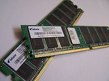
![]()
Модули ОЗУ для ПК

![]()
Простейшая схема взаимодействия оперативной памяти с ЦП
Операти́вная па́мять (англ. Random Access Memory, память с произвольным доступом; комп. жарг. Память, Оперативка, Мозги) — энергозависимая часть системы компьютерной памяти, в которой временно хранятся данные и команды, необходимые процессору для выполнения им операции. Обязательным условием является адресуемость (каждое машинное слово имеет индивидуальный адрес) памяти[источник не указан 128 дней].
Обмен данными между процессором и оперативной памятью производится:
- непосредственно,
- либо через сверхбыструю память, 0-го уровня — регистры в АЛУ, либо при наличии кэша — через него.
Содержащиеся в оперативной памяти данные доступны только тогда, когда на модули памяти подаётся напряжение, то есть, компьютер включён. Пропадание на модулях памяти питания, даже кратковременное, приводит к искажению либо полному уничтожению данных в ОЗУ.
Энергосберегающие режимы работы материнской платы компьютера позволяют переводить его в режим «сна», что значительно сокращает уровень потребления компьютером электроэнергии. Для сохранения содержимого ОЗУ в таком случае, применяют запись содержимого оперативной памяти в специальный файл (в системе Windows XP он называется hiberfil.sys).
В общем случае, оперативная память содержит данные операционной системы и запущенных на выполнение программ, поэтому от объёма оперативной памяти зависит количество задач, которые одновременно может выполнять компьютер.
Оперативное запоминающее устройство, ОЗУ — техническое устройство, реализующее функции оперативной памяти.
ОЗУ может изготавливаться как отдельный блок или входить в конструкцию, например однокристальной ЭВМ или микроконтроллера.
Содержание
- 1 История
- 2 ОЗУ современных компьютеров
- 2.1 Память динамического типа (англ. DRAM (Dynamic Random Access Memory))
- 2.2 Память статического типа (англ. SRAM (Static Random Access Memory))
- 3 Логическая структура памяти в IBM PC
- 4 См. также
- 5 Литература
- 6 Ссылки
История
В 1834 году Чарльз Бэббидж начал разработку Аналитической машины. Одна из важных частей этой машины называлась «Склад» (store), и предназначалась для хранения промежуточных результатов вычислений. Результаты запоминались с использованием валов и шестерней.
ЭВМ первого поколения можно считать ещё экспериментальными, поэтому в них использовалось множество разновидностей запоминающих устройств: на ртутных линиях задержки, электронно-лучевых и электростатических трубках. В качестве оперативной памяти использовался также магнитный барабан: он обеспечивал достаточное для компьютеров тех времён быстродействие и использовался в качестве основной памяти для хранения программ и вводимых данных.
Второе поколение требовало более технологичных в производстве схем оперативной памяти. Наиболее распространённым видом памяти в то время стала память на магнитных сердечниках.
Начиная с третьего поколения большинство узлов компьютеров стали выполнять на микросхемах, в том числе и оперативную память. Наибольшее распространение получили два вида ОЗУ: на основе конденсаторов (динамическая память) и триггеров (статическая память). Оба этих вида памяти не способны сохранять данные при отключении питания — для этой цели используется Энергонезависимая память.
ОЗУ современных компьютеров
ОЗУ большинства современных компьютеров представляет собой модули динамической памяти, содержащие полупроводниковые ИС ЗУ, организованные по принципу устройств с произвольным доступом. Память динамического типа дешевле, чем статического, и её плотность выше, что позволяет на том же пространстве кремниевой подложки размещать больше ячеек памяти, но при этом её быстродействие ниже. Статическая, наоборот, более быстрая память, но она и дороже. В связи с этим массовую оперативную память строят на модулях динамической памяти, а память статического типа используется для построения кеш-памяти внутри микропроцессора.
Память динамического типа (англ. DRAM (Dynamic Random Access Memory))
Основная статья: DRAM
Экономичный вид памяти. Для хранения разряда (бита или трита) используется схема, состоящая из одного конденсатора и одного транзистора (в некоторых вариациях конденсаторов два). Такой вид памяти решает, во-первых, проблему дороговизны (один конденсатор и один транзистор дешевле нескольких транзисторов) и во-вторых, компактности (там, где в SRAM размещается один триггер, то есть один бит, можно уместить восемь конденсаторов и транзисторов). Есть и свои минусы. Во-первых, память на основе конденсаторов работает медленнее, поскольку если в SRAM изменение напряжения на входе триггера сразу же приводит к изменению его состояния, то для того чтобы установить в единицу один разряд (один бит) памяти на основе конденсатора, этот конденсатор нужно зарядить, а для того чтобы разряд установить в ноль, соответственно, разрядить. А это гораздо более длительные операции (в 10 и более раз), чем переключение триггера, даже если конденсатор имеет весьма небольшие размеры. Второй существенный минус — конденсаторы склонны к «стеканию» заряда; проще говоря, со временем конденсаторы разряжаются. Причём разряжаются они тем быстрее, чем меньше их ёмкость.
За то, что разряды в ней хранятся не статически, а «стекают» динамически во времени, память на конденсаторах получила своё название динамическая память. В связи с этим обстоятельством, дабы не потерять содержимое памяти, заряд конденсаторов для восстановления необходимо «регенерировать» через определённый интервал времени. Регенерация выполняется центральным микропроцессором или контроллером памяти, за определённое количество тактов считывания при адресации по строкам. Так как для регенерации памяти периодически приостанавливаются все операции с памятью, это значительно снижает производительность данного вида ОЗУ.
Память статического типа (англ. SRAM (Static Random Access Memory))
ОЗУ, которое не надо регенерировать (и обычно схемотехнически собранное на триггерах), называется статической памятью с произвольным доступом или просто статической памятью. Достоинство этого вида памяти — скорость. Поскольку триггеры собраны на вентилях, а время задержки вентиля очень мало, то и переключение состояния триггера происходит очень быстро. Данный вид памяти не лишён недостатков. Во-первых, группа транзисторов, входящих в состав триггера, обходится дороже, даже если они вытравляются миллионами на одной кремниевой подложке. Кроме того, группа транзисторов занимает гораздо больше места, поскольку между транзисторами, которые образуют триггер, должны быть вытравлены линии связи. Используется для организации сверхбыстрого ОЗУ, критичного к скорости работы.
Логическая структура памяти в IBM PC
См. также: x86
В реальном режиме память делится на следующие участки:
- Основная область памяти (англ. conventional memory).
- Расширенная память (EMS)
- Дополнительная память (XMS)
- Upper Memory Area (UMA)
- High Memory Area (HMA)
См. также
- Запоминающее устройство с произвольным доступом
- Прямой доступ к памяти
- Вычислительный конвейер
- Магниторезистивная оперативная память
- Троичная ячейка памяти
- Советские микросхемы для построения запоминающих устройств
Литература
- Скотт Мюллер. Глава 6. Оперативная память // Модернизация и ремонт ПК = Upgrading and Repairing PCs. — 17-е изд. — М.: Вильямс, 2007. — С. 499—572. — ISBN 0-7897-3404-4
- Под. ред. чл.-корр. АН УССР Б. Н. Малиновского. Глава 2.3 БИС ЗУ для построения внутренней памяти // Справочник по персональным ЭВМ. — К.: Тэхника, 1990. — С. 384. — ISBN 5-335-00168-2
Ссылки
- Современная оперативная память (RAM FAQ 1.01)
| |
|
|---|---|
| Системный блок |
Блок питания • Охлаждение • Материнская плата • Процессор • Шины • Видеокарта • Звуковая карта • Сетевая плата |
| Память |
Оперативная память • Запоминающее устройство с произвольным доступом |
| Носители и дисководы |
Жёсткий диск • Твердотельный накопитель (Флеш-память • USB-флеш) • Оптический привод (CD • DVD • BD) • НГМД (Дискета) • Стример • Кардридер |
| Вывод |
Динамик • Монитор • Принтер • Графопостроитель (плоттер) Акустическая система • |
| Ввод |
Клавиатура • Мышь • Трекбол • TrackPoint • Тачпад • Сенсорный экран • Цифровая ручка • Световое перо • Графический планшет • Микрофон • Сканер • Веб-камера |
| Игры |
Джойстик • Руль • Штурвал • Педали • Пистолет • Paddle • Геймпад • Дэнспад • Трекер |
| Прочее |
Модем • ТВ-тюнер • Сетевой фильтр • ИБП |
Содержание
- Значение словосочетания «оперативная память»
-
- Делаем Карту слов лучше вместе
-
Значение словосочетания «оперативная память»
- Операти́вная па́мять (англ. Random Access Memory, RAM, память с произвольным доступом) или операти́вное запомина́ющее устро́йство (ОЗУ); комп. жарг. па́мять, операти́вка — энергозависимая часть системы компьютерной памяти, в которой во время работы компьютера хранится выполняемый машинный код (программы), а также входные, выходные и промежуточные данные, обрабатываемые процессором.
Обмен данными между процессором и оперативной памятью производится:
через сверхбыструю память 0-го уровня — регистры в АЛУ, либо при наличии аппаратного кэша процессора — через кэш.
Содержащиеся в современной полупроводниковой оперативной памяти данные доступны и сохраняются только тогда, когда на модули памяти подаётся напряжение. Выключение питания оперативной памяти, даже кратковременное, приводит к искажению либо полному разрушению хранимой информации.
Энергосберегающие режимы работы материнской платы компьютера позволяют переводить его в режим сна, что значительно сокращает уровень потребления компьютером электроэнергии. В режиме гибернации питание ОЗУ отключается. В этом случае для сохранения содержимого ОЗУ операционная система (ОС) перед отключением питания записывает содержимое ОЗУ на устройство постоянного хранения данных (как правило, жёсткий диск). Например, в ОС Windows XP содержимое памяти сохраняется в файл hiberfil.sys, в ОС семейства Unix — на специальный swap-раздел жёсткого диска.
В общем случае, ОЗУ содержит программы и данные ОС и запущенные прикладные программы пользователя и данные этих программ, поэтому от объёма оперативной памяти зависит количество задач, которые одновременно может выполнять компьютер под управлением ОС.
Оперативное запоминающее устройство, ОЗУ — техническое устройство, реализующее функции оперативной памяти.
ОЗУ может изготавливаться как отдельный внешний модуль или располагаться на одном кристалле с процессором, например, в однокристальных ЭВМ или однокристальных микроконтроллерах.
Делаем Карту слов лучше вместе
Привет! Меня зовут Лампобот, я компьютерная программа, которая помогает делать Карту слов. Я отлично умею считать, но пока плохо понимаю, как устроен ваш мир. Помоги мне разобраться!
Спасибо! Я обязательно научусь отличать широко распространённые слова от узкоспециальных.
Насколько понятно значение слова подхват (существительное):
Изучая технические характеристики компьютеров, пользователи часто сталкиваются с непонятными аббревиатурами или терминами. Яркий пример, аббревиатуры ОЗУ или RAM. Обычно производители и продавцы компьютеров указывают что-то вроде «ОЗУ – 8 Гб» или «RAM – 8 Гб». При этом данные аббревиатуры никак не расшифровываются и не объясняются, предполагается, что покупатели должны знать, что они означают. Но, это далеко не всегда так. В данной статье мы расскажем о том, что такое ОЗУ или RAM в компьютере и для чего они используются.
Начнем с главного, аббревиатуры ОЗУ и RAM обозначают одно и тоже, а именно оперативную память. ОЗУ расшифровывается как оперативное запоминающее устройство, а RAM как Random Access Memory, что переводится как запоминающее устройство с произвольным доступом и означает тоже самое. Поэтому, если в характеристиках компьютера написано «ОЗУ – 8 Гб» или «RAM – 8 Гб», то это означает что объем оперативной памяти данного компьютера составляет 8 Гб.
Теперь чуть подробней о том, что такое ОЗУ в компьютере и для чего она нужна. ОЗУ или проще говоря оперативная память – это энергозависимая память, в которой хранятся данные и команды, которые обрабатываются процессором. Энергозависимая означает, что она работает только при наличии электропитания. Как только питание пропадает, все данные из оперативной памяти удаляются. Именно поэтому оперативная память не может использоваться для долговременного хранения данных.
За время развития компьютеров появилось не мало различных типов ОЗУ, которые работают на основе разных физических принципов. В современных компьютерах уже достаточно давно используется память типа DDR SD RAM или Double Data Rate Synchronous Dynamic Random Access Memory, что можно перевести как синхронная динамическая память с произвольным доступом и удвоенной скоростью передачи данных. Сейчас актуальным стандартом является DDR4 – это четвертое поколение оперативной памяти DDR SD RAM и большинство новых компьютеров поставляются именно с DDR4.
Память DDR – это небольшая плата с чипами, которая подключается к специальным слотам на материнской плате компьютера. Обычно такие слоты находятся справа от процессора в количестве двух или четырех штук. На самых продвинутых материнских платах таких слотов может быть шесть или восемь и в этом случае они размещаются по обе стороны от процессора. Модули DDR разных поколений не совместимы друг с другом. Поэтому, установить DDR4 в материнскую плату с поддержкой DDR3 не получится.
На картинке внизу показаны модули оперативной памяти от DDR до DDR4. Как можно заметить, у них есть специальная прорезь (ключ), которая препятствует установке памяти в не подходящую материнскую плату.

Также нужно отметить, что оперативная память для ноутбуков конструктивно отличается от оперативной памяти для настольных компьютеров. Поэтому установить память для ноутбука в настольный компьютер или наоборот также не получится.
Посмотрите также:
- Как узнать частоту оперативной памяти
- Как подобрать оперативную память для компьютера
- Как посмотреть, сколько оперативной памяти на компьютере
- Как добавить оперативной памяти в компьютер
- Как проверить оперативную память компьютера
Автор
Александр Степушин
Создатель сайта comp-security.net, автор более 2000 статей о ремонте компьютеров, работе с программами, настройке операционных систем.
Остались вопросы?
Задайте вопрос в комментариях под статьей или на странице
«Задать вопрос»
и вы обязательно получите ответ.
У оперативной памяти много названий. Оперативное запоминающее устройство (ОЗУ) определяет назначение — запоминать и хранить временную информацию, требующуюся процессору при выполнении операций. Английская аббревиатура RAM (Random Access Memory) означает память с произвольным доступом, то есть запрос к требуемой ячейке памяти происходит напрямую, другие блоки не затрагиваются. Также этот вид памяти называют энергозависимым, а значит, данные сохраняются в ней до тех пор, пока включено устройство, в котором она установлена. В разговорах ИТ-специалистов фигурирует слово «оперативка», но чаще всего это просто «память»: компьютера, телефона, серверная и т.п. Разберем, для чего нужна оперативная память, рассмотрим наиболее важные характеристики, влияющие на быстродействие и производительность и заслуживающие внимания при выборе, а также коснемся особенностей серверного ОЗУ.
Функции оперативной памяти
В компьютере помимо оперативного установлено и постоянное запоминающее устройство — ПЗУ, более известное как жесткий диск или винчестер. Это энергонезависимый тип памяти, который сохраняет всю информацию даже после отключения питания компьютера. Для выполнения работы центральному процессору требуется информация, хранящаяся на жестком диске. Данные копируются с винчестера в своеобразный буфер, которым и является оперативная память, а по окончании работы, после сохранения (если требуется) измененных данных обратно на винчестер, ОЗУ очищается. Кроме процессора информацию, хранящуюся в оперативной памяти, с целью быстродействия могут использовать другие компоненты системы — видеокарта и т.д.
Итак, оперативная память ускоряет процесс взаимодействия ЦПУ с винчестером, и соответственно приводит к увеличению производительности оборудования в целом. Поэтому важно понимать, какие именно параметры оперативной памяти позволят добиться наибольшей эффективности, а при каких условиях система вовсе не станет функционировать.
Типы памяти
Статическая память (SRAM — Static RAM) — быстрая, но не дешевая, часто находит применение в кэш-памяти процессоров, видеокарт и т.п.
Динамическая память (DRAM — Dynamic RAM) — не такая быстрая, как статическая, но зато более дешевая и находит повсеместное применение в компьютерах и других устройствах, поэтому о ней расскажем подробнее.
Широко распространены поколения динамической памяти DDR SDRAM (англ. Double Data Rate Synchronous DRAM), характеризующиеся удвоенной скоростью передачи данных:
- DDR SDRAM
- DDR2 SDRAM
- DDR3 SDRAM
- DDR4 SDRAM
Отличаются между собой количеством контактов, разъемом, повышением производительности и снижением потребления электроэнергии от поколения к поколению. На сегодня самыми популярными являются модули DDR3 и DDR4.
Частота функционирования
Параметр, характеризующий передачу данных между ОЗУ и процессором за единицу времени, — частота — также влияет на быстродействие системы. Высокий показатель означает большее количество переданной информации. Измеряется в мегагерцах и пишется рядом с типом памяти: DDR3-1200, где 1200 (МГц) — это частота передачи данных.
Пропускная способность
Быстродействие системы зависит также от пропускной способности ОЗУ — объема информации, обрабатываемой за единицу времени. Измеряется в мегабайтах в секунду, в характеристиках планки памяти обозначается так: PC3-10600, где 10600 (МБ/с) — максимально возможная скорость обработки данных.
Тайминги
Другой показатель, влияющий на производительность вычислительного устройства, характеризуется временем отсрочки выполнения команд оперативной памятью — таймингами (латентностью), ответственными за подготовку памяти к работе во избежание искажения данных. Чем ниже показатель тайминга, тем продуктивнее ОЗУ. На планке памяти маркируются либо 4 типа таймингов (2-2-3-6), либо первое из значений (CL2).
Объем оперативной памяти
Одной из главных характеристик, на которую чаще всего ориентируются при выборе оперативной памяти, является ее объем, измеряемый в мегабайтах и гигабайтах. Очевидно, что чем больше объем оперативной памяти, тем быстрее будет работа компьютера. Но есть нюансы. Во-первых, количество и тип слотов на материнской плате физически ограничивает число и тип планок памяти, которые можно установить в компьютер. А во-вторых, даже если взять модули максимального объема, от разрядности процессора зависит, будут ли в полной мере использоваться все эти гигабайты, или же деньги потрачены впустую. Дело в том, что 32-разрядные процессоры поддерживают не более 4 ГБ ОЗУ. 64-разрядные ЦПУ могут работать и с большим объемом.
Особо следует отметить, что при выборе парных планок оперативной памяти важно, чтобы все параметры были одинаковые, иначе система будет функционировать с наименьшими значениями или не будет работать вовсе. Кроме того, необходимо учитывать, какие модули памяти поддерживают процессор и материнская плата.
Серверная оперативная память
Помимо максимальной производительности и быстродействия, от памяти для сервера требуется высокая надежность и бесперебойная работа. Возникающие в процессе непрерывной работы случайные ошибки отрицательно воздействуют на производительность сервера и могут приводить к потере данных. Чтобы избежать этого, в ОЗУ для сервера обязательно применяется технология ECC (Error Correcting Code) — исправление наиболее вероятных ошибок путем избыточного кодирования информации.
Планки памяти, поддерживающие технологию коррекции ошибок, имеют добавочные микросхемы, содержащие ECC-код. Из-за этого цена серверной оперативной памяти возрастает. Материнская плата, чипсет и процессор должны поддерживать модули ECC-памяти, что тоже оказывает влияние на увеличение общей стоимости оборудования.
Еще один тип серверной памяти — буферизованная, или регистровая память. На планке имеется одна или более микросхем регистров для буферизации данных, поступающих от контроллера памяти. Такая конструктивная особенность снижает нагрузку на контроллер, благодаря чему можно установить большее количество модулей памяти.
Вы можете выбрать выделенные серверы от ATLEX.Ru, предлагаемые в аренду в России или в Европе, по объему памяти, необходимой для ваших нужд. А если вас устраивают прочие параметры сервера, но хочется больше производительности, то всегда можно установить дополнительные модули по вашему желанию.

Анастасия Николаевна Королева
Эксперт по предмету «Информатика»
Задать вопрос автору статьи
Определение 1
Оперативная память (ОЗУ, $Random Access Memory$ – $RAM$, память с произвольным доступом) – запоминающее устройство сравнительно небольшого объёма, которое непосредственно связано с ЦП и предназначено для записи, чтения и хранения данных о выполняемых программах и данных, обрабатываемых этими программами.
Оперативная память используется только для временного хранения данных и программ, т.к. при выключении ПК информация, которая находилась в ОЗУ, пропадает. Доступ к элементам оперативной памяти прямой, т.е. каждый байт памяти имеет свой индивидуальный адрес.
Назначение ОЗУ
Замечание 1
Оперативная память используется для хранения и передачи информации ЦП, на жесткий диск, на другие внешние устройства, которая располагается в специальных разъемах на материнской плате. ОЗУ представляет собой схему из огромного числа мельчайших конденсаторов и транзисторов (одна пара позволяет хранить $1$ бит). При выключении ПК введенная информация исчезает, т.к. данные не были записаны на жесткий диск, где могут долго сохраняться, а находились в ОЗУ. Но в случае отсутствия оперативной памяти, данные должны были бы располагаться на жестком диске, и тогда время обращения к ним резко бы увеличилось, что привело бы к резкому снижению общей производительности ПК.
Итак, ОЗУ используется для:
- хранения данных и команд для дальнейшей их передачи ЦП для обработки;
- хранение результатов вычислений, которые были произведены ЦП.
- считывание (или запись) содержимого ячеек.
Оперативная память изготовлена в виде микросхем, которые крепятся на специальных пластинах и устанавливаются на системной плате в соответствующие разъемы.
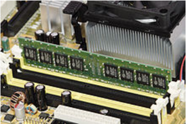
Рисунок 1. Модуль оперативной памяти, вставленный в системную плату
При включении ПК в ОЗУ загружается операционная система, затем программное обеспечение и документы. ЦП управляет загрузкой программ и данных в ОЗУ, далее данные в ОЗУ обрабатываются. Таки образом, ЦП работает с инструкциями и данными, которые находятся в ОЗУ, а другие устройства (диски, магнитная лента, модем и т.д.) действуют через нее. Поэтому оперативная память имеет огромное влияние на работу компьютера. Т.к. ОЗУ предназначена для хранения данных и программ только во время работы ПК, то после выключения электропитания все данные в ОЗУ теряются. Во избежание потери данных или внесенных в документы изменений перед выключением ПК необходимо сохранить данные на жесткий диск и только потом выйти из приложения.
«Оперативная память» 👇
Типы оперативной памяти
Выделяют $2$ вида оперативной памяти:
- статическую ($SRAM$) – используется в качестве кэш-памяти ЦП;
- динамическую ($DRAM$) – используется в качестве оперативной памяти ПК.
Ячейки динамической памяти можно представить в виде микроконденсаторов, которые способны накапливать электрический заряд. Недостатками $DRAM$-памяти является более низкая скорость записи и чтения данных и необходимость постоянной подзарядки.
Основными являются виды типа $SDRAM$ ($Synchronous Dynamic Random Access Memory$ – синхронная динамическая память с произвольным доступом):
$DDR$ ($Double Data Rate$ – двойная скорость передачи данных). Удвоенная скорость достигается за счет считывания данных по нарастанию и по спаду сигнала.
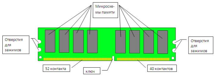
Рисунок 2. Схема платы памяти DDR
На плате оперативной памяти (рис. 2) с обеих сторон находятся микросхемы с памятью. Снизу находится ключ для вставки платы в разъем системной платы.
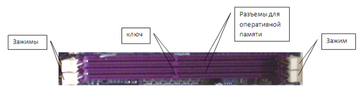
Рисунок 3. Разъемы для установки оперативной памяти
$DDR2$ от $DDR$ отличается удвоенной частотой шины, по которой данные передаются в буфер, и способность работы на более высокой частоте. Скорость работы $DDR2$ чуть выше, чем у $DDR$.
$DDR3$ отлична от $DDR2$ пониженным энергопотреблением (на $40 %$).
$DDR4$ отличается повышенными частотными характеристиками и пониженным напряжением питания.
Платы $DDR$, $DDR2$, $DDR3$ и $DDR4$ не являются взаимозаменяемыми, т.к. имеют различия в строении (смещение ключа, разное количество контактов и т.п.).
Основные характеристики ОЗУ
Основные характеристики:
- Объем памяти – максимальное количество информации, которая может быть помещена в эту память, выражается в Кб, Мб и Гб.
- Время доступа к памяти (в наносекундах) представляет собой минимальное время, необходимое для размещения в памяти единицы информации.
- Плотность записи (в $бит/см^2$) – количество информации, которая записана на единице поверхности носителя.
$SIMM$-модули имеют объем $4$, $8$, $16$, $32$, $64$ Мб; $DIMM$-модули – $16$, $32$, $64$, $128$, $256$, $512$ Мб.
Время доступа SIMM-модулей – $50–70$ нс, $DIMM$-модулей – $7–10$ нс.
Модули оперативной памяти
Оперативная память в ПК размещена на стандартных панелях, которые называют модулями. Модули памяти представлены в двух видах:
- односторонне расположение выводов ($SIMM$-модули) можно устанавливать только парами;
- двухстороннее расположение выводов ($DIMM$-модули) можно устанавливать по одному, обладают большей скоростью передачи.
Устанавливать на одной плате разные модули нельзя.
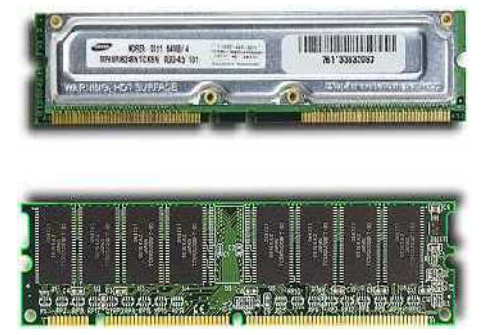
Рисунок 4. Микросхемы памяти SIMM (сверху) и DIMM (снизу)
Находи статьи и создавай свой список литературы по ГОСТу
Поиск по теме